Electrical Specifications
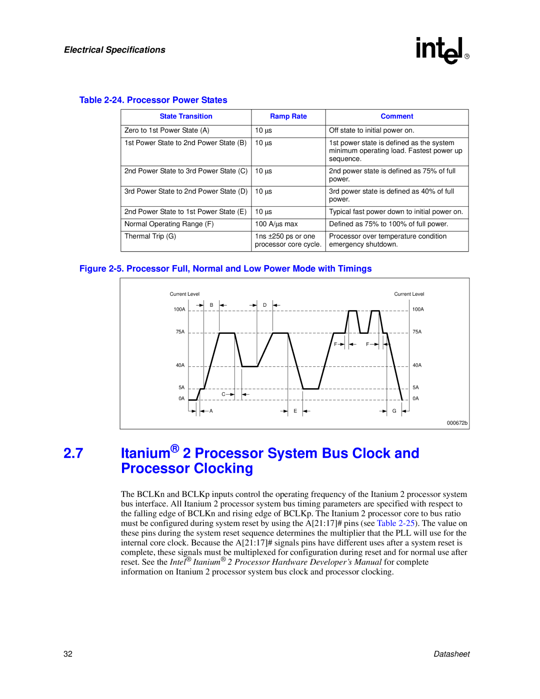
Table 2-24. Processor Power States
State Transition | Ramp Rate | Comment |
|
|
|
Zero to 1st Power State (A) | 10 μs | Off state to initial power on. |
|
|
|
1st Power State to 2nd Power State (B) | 10 μs | 1st power state is defined as the system |
|
| minimum operating load. Fastest power up |
|
| sequence. |
|
|
|
2nd Power State to 3rd Power State (C) | 10 μs | 2nd power state is defined as 75% of full |
|
| power. |
|
|
|
3rd Power State to 2nd Power State (D) | 10 μs | 3rd power state is defined as 40% of full |
|
| power. |
|
|
|
2nd Power State to 1st Power State (E) | 10 μs | Typical fast power down to initial power on. |
|
|
|
Normal Operating Range (F) | 100 A/μs max | Defined as 75% to 100% of full power. |
|
|
|
Thermal Trip (G) | 1ns ±250 ps or one | Processor over temperature condition |
| processor core cycle. | emergency shutdown. |
|
|
|
Figure 2-5. Processor Full, Normal and Low Power Mode with Timings
Current Level
100A
75A
40A
5A
0A
B
C
A
D
E
F
F
Current Level
100A
75A
40A
5A
0A
G
000672b
2.7Itanium® 2 Processor System Bus Clock and Processor Clocking
The BCLKn and BCLKp inputs control the operating frequency of the Itanium 2 processor system bus interface. All Itanium 2 processor system bus timing parameters are specified with respect to the falling edge of BCLKn and rising edge of BCLKp. The Itanium 2 processor core to bus ratio must be configured during system reset by using the A[21:17]# pins (see Table
32 | Datasheet |