Electrical Specifications
Table
|
| System |
|
|
|
|
|
| |
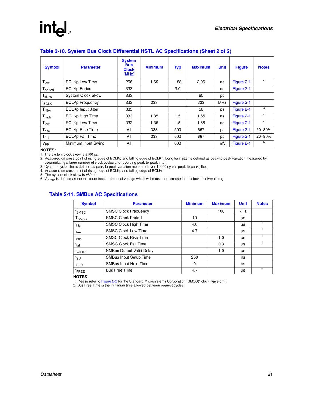
Symbol | Parameter | Bus | Minimum | Typ | Maximum | Unit | Figure | Notes | |
Clock | |||||||||
|
|
|
|
|
|
|
| ||
|
| (MHz) |
|
|
|
|
|
| |
|
|
|
|
|
|
|
|
| |
Tlow | BCLKp Low Time | 266 | 1.69 | 1.88 | 2.06 | ns | Figure | 4 | |
| |||||||||
Tperiod | BCLKp Period | 333 |
| 3.0 |
| ns | Figure |
| |
Tskew | System Clock Skew | 333 |
|
| 60 | ps |
|
| |
fBCLK | BCLKp Frequency | 333 | 333 |
| 333 | MHz | Figure |
| |
Tjitter | BCLKp Input Jitter | 333 |
|
| 50 | ps | Figure | 3 | |
|
|
| |||||||
Thigh | BCLKp High Time | 333 | 1.35 | 1.5 | 1.65 | ns | Figure | 4 | |
| |||||||||
Tlow | BCLKp Low Time | 333 | 1.35 | 1.5 | 1.65 | ns | Figure | 4 | |
| |||||||||
Trise | BCLKp Rise Time | All | 333 | 500 | 667 | ps | Figure | ||
Tfall | BCLKp Fall Time | All | 333 | 500 | 667 | ps | Figure | ||
VPP | Minimum Input Swing | All |
| 600 |
| mV | Figure | 6 | |
|
|
|
NOTES:
1.The system clock skew is ±100 ps.
2.Measured on cross point of rising edge of BCLKp and falling edge of BCLKn. Long term jitter is defined as
3.
4.Measured on cross point of rising edge of BCLKp and falling edge of BCLKn.
5.The system clock skew is ±60 ps.
6.VPPmin is defined as the minimum input differential voltage which will cause no increase in the clock receiver timing.
Table 2-11. SMBus AC Specifications
Symbol | Parameter | Minimum | Maximum | Unit | Notes |
|
|
|
|
|
|
fSMSC | SMSC Clock Frequency |
| 100 | kHz |
|
TSMSC | SMSC Clock Period | 10 |
| µs |
|
thigh | SMSC Clock High Time | 4.0 |
| µs | 1 |
|
| ||||
tlow | SMSC Clock Low Time | 4.7 |
| µs | 1 |
|
| ||||
trise | SMSC Clock Rise Time |
| 1.0 | µs | 1 |
|
| ||||
tfall | SMSC Clock Fall Time |
| 0.3 | µs | 1 |
|
| ||||
tVALID | SMBus Output Valid Delay |
| 1.0 | µs |
|
tSU | SMBus Input Setup Time | 250 |
| ns |
|
tHLD | SMBus Input Hold Time | 0 |
| ns |
|
tFREE | Bus Free Time | 4.7 |
| µs | 2 |
|
|
NOTES:
1.Please refer to Figure
2.Bus Free Time is the minimum time allowed between request cycles.
Datasheet | 21 |