System Management Feature Specifications
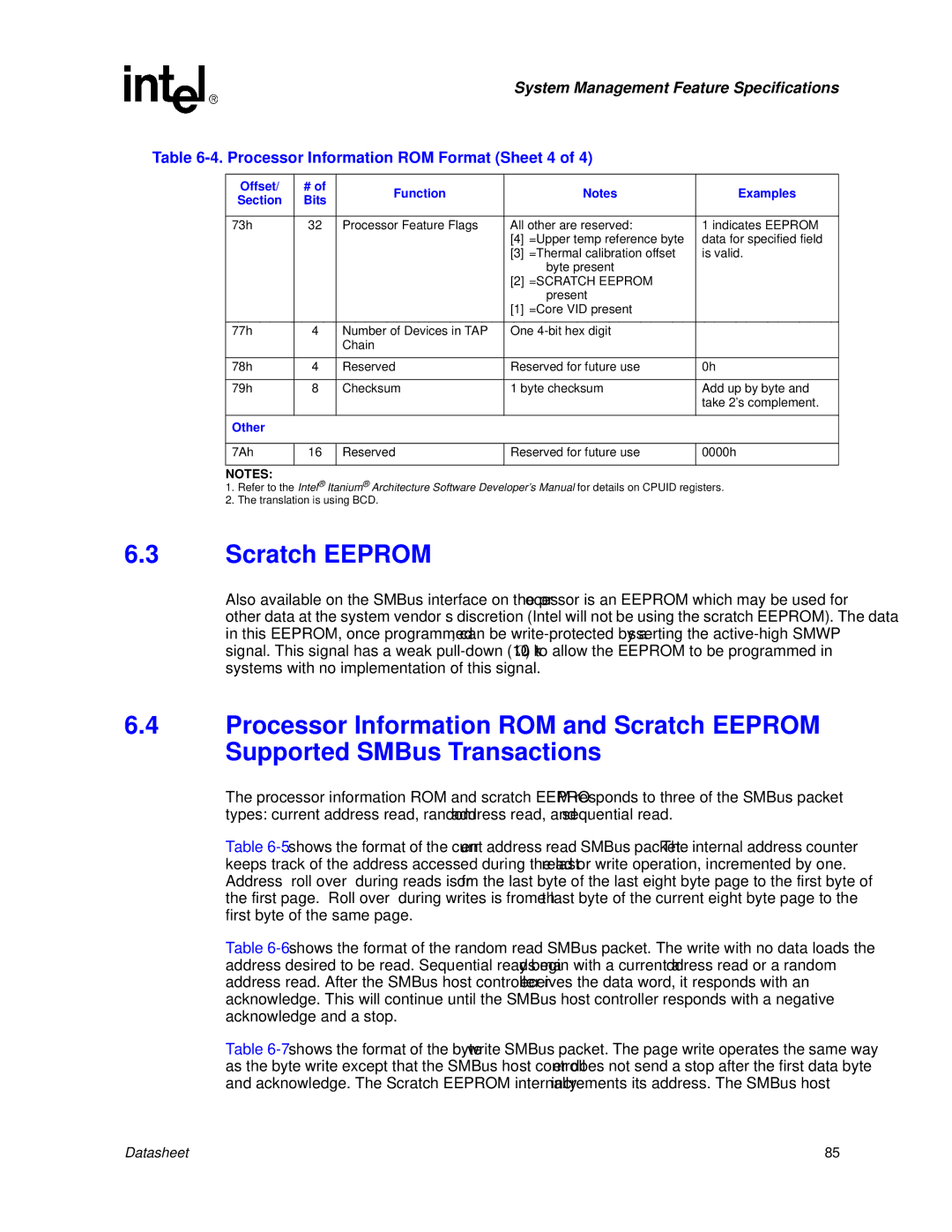
Table 6-4. Processor Information ROM Format (Sheet 4 of 4)
Offset/ | # of | Function |
| Notes | Examples |
Section | Bits |
| |||
|
|
|
| ||
|
|
|
|
| |
73h | 32 | Processor Feature Flags | All other are reserved: | 1 indicates EEPROM | |
|
|
| [4] | =Upper temp reference byte | data for specified field |
|
|
| [3] | =Thermal calibration offset | is valid. |
|
|
|
| byte present |
|
|
|
| [2] | =SCRATCH EEPROM |
|
|
|
|
| present |
|
|
|
| [1] | =Core VID present |
|
|
|
|
|
| |
77h | 4 | Number of Devices in TAP | One |
| |
|
| Chain |
|
|
|
|
|
|
|
| |
78h | 4 | Reserved | Reserved for future use | 0h | |
|
|
|
|
| |
79h | 8 | Checksum | 1 byte checksum | Add up by byte and | |
|
|
|
|
| take 2’s complement. |
|
|
|
|
|
|
Other |
|
|
|
|
|
|
|
|
|
| |
7Ah | 16 | Reserved | Reserved for future use | 0000h | |
|
|
|
|
|
|
NOTES:
1.Refer to the Intel® Itanium® Architecture Software Developer’s Manual for details on CPUID registers.
2.The translation is using BCD.
6.3Scratch EEPROM
Also available on the SMBus interface on the processor is an EEPROM which may be used for other data at the system vendor’s discretion (Intel will not be using the scratch EEPROM). The data in this EEPROM, once programmed, can be
6.4Processor Information ROM and Scratch EEPROM Supported SMBus Transactions
The processor information ROM and scratch EEPROM responds to three of the SMBus packet types: current address read, random address read, and sequential read.
Table
Table
Table
Datasheet | 85 |