Signals Reference
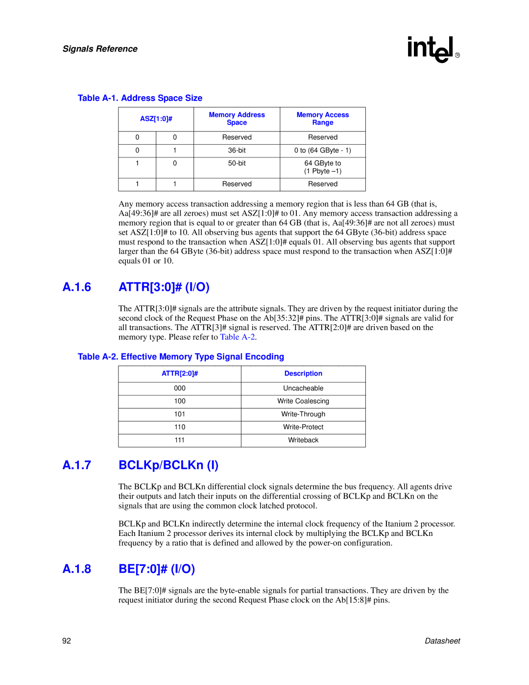
Table A-1. Address Space Size
| ASZ[1:0]# | Memory Address | Memory Access | |
| Space | Range | ||
|
|
| ||
|
|
|
| |
0 |
| 0 | Reserved | Reserved |
|
|
|
|
|
0 |
| 1 | 0 to (64 GByte - 1) | |
|
|
|
|
|
1 |
| 0 | 64 GByte to | |
|
|
|
| (1 Pbyte |
|
|
|
|
|
1 |
| 1 | Reserved | Reserved |
|
|
|
|
|
Any memory access transaction addressing a memory region that is less than 64 GB (that is, Aa[49:36]# are all zeroes) must set ASZ[1:0]# to 01. Any memory access transaction addressing a memory region that is equal to or greater than 64 GB (that is, Aa[49:36]# are not all zeroes) must set ASZ[1:0]# to 10. All observing bus agents that support the 64 GByte
A.1.6 ATTR[3:0]# (I/O)
The ATTR[3:0]# signals are the attribute signals. They are driven by the request initiator during the second clock of the Request Phase on the Ab[35:32]# pins. The ATTR[3:0]# signals are valid for all transactions. The ATTR[3]# signal is reserved. The ATTR[2:0]# are driven based on the memory type. Please refer to Table
Table A-2. Effective Memory Type Signal Encoding
ATTR[2:0]# | Description |
|
|
000 | Uncacheable |
|
|
100 | Write Coalescing |
|
|
101 | |
|
|
110 | |
|
|
111 | Writeback |
|
|
A.1.7 BCLKp/BCLKn (I)
The BCLKp and BCLKn differential clock signals determine the bus frequency. All agents drive their outputs and latch their inputs on the differential crossing of BCLKp and BCLKn on the signals that are using the common clock latched protocol.
BCLKp and BCLKn indirectly determine the internal clock frequency of the Itanium 2 processor. Each Itanium 2 processor derives its internal clock by multiplying the BCLKp and BCLKn frequency by a ratio that is defined and allowed by the
A.1.8 BE[7:0]# (I/O)
The BE[7:0]# signals are the
92 | Datasheet |
