UG068 v1.01 August 25
ML310 User Guide
ML310 User Guide
Version Revision
ML310 User Guide UG068 v1.01 August 25
UG068 v1.01 August 25
Table of Contents
UG068 v1.01 August 25
Additional Resources
Manual Contents
Typographical
Conventions
Handbook
Online Document
Chapter
Virtex-II Pro
Summary of Virtex-II Pro Features
RocketIO 3.125 Gb/s Transceivers
PowerPC 405 Core
Virtex-II Pro
Virtex-II Fpga Fabric
Foundation ISE
Foundation Features
Design Entry
Introduction to Virtex-II Pro, ISE, and EDK
Implementation and Configuration
Synthesis
Foundation ISE
Board Level Integration
Embedded Development Kit
Overview
ML310 Embedded Development Platform
ML310 Board
ML310 Embedded Development Platform
Overview
Features
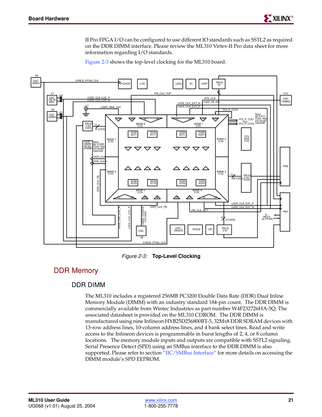
Clock Generation
Board Hardware
Board Hardware
DDR Memory
DDR Signaling
DDR Memory Expansion
U37
DDRA2
DDRDQS02
DDRDQ31
Serial Port Fpga Uart
Signaling Standards of RS-232
Introduction to Serial Ports
RS-232 on the ML310
Board Bring-Up
System ACE CF Controller
XC2VP30 Connectivity
Non-Volatile Storage
6JTAG Connections to the XC2VP30 and System ACE
Jtag Connection to XC2VP30
System ACE Jtag Configuration Interface
Gpio LEDs and LCD
Parallel Cable IV Interface
8LEDs and LCD Connectivity
Gpio LED Interface
UCF Signal Name Translator U37 J13 U35
Gpio LCD Interface
U37 Name U36
CPU Debug and CPU Trace
CPU Debug Description
Buffer U33 J13
9Combined Trace/Debug Connector Pinout
CPU Debug Connector Pinout
PCI Bus
CPU Debug Connection to XC2VP30
ML310 Embedded Development Platform
11 PCI Bus and Device Connectivity
Pciinta Pciintb Pciintc
Pcipar Pcippar Pcirstn Pciprstn
113.3V Primary PCI Bus Information Device Vendor
ALi South Bridge Interface, M1535D+, U15
Device Name Bus
125.0V Secondary PCI Bus Information Device Name Vendor
12ALi South Bridge Interface, M1535D+, U15
Parallel Port Interface, connector assembly P1
Serial Port Interface, connector assembly P1
USB, connector assembly J3
IDE, connectors J15 and J16
GPIO, connector J5
System Management Bus SMBus
17Type of Gpio Available on Header J5 ALi Gpio Types Number
AC97 Audio
19Audio Jacks, J1 and J2 Signal name Description
Flash ROM, U4
PS/2 Keyboard/Mouse Interface, connector P2
Intel GD82559 Ethernet Controller
Intel GD82559, U11, 10/100 Ethernet Controller
IIC/SMBus Interface
IIC/SMBus Signaling
Introduction to IIC/SMBus
IIC/SMBus on ML310 Board
22shows the Fpga connections to all SMBus and IIC devices
14SMBus and IIC Block Diagram
Serial Peripheral Interface SPI
SPI Signaling
Push Buttons, Switches, Front Panel Interface and Jumpers
SPI Addressing
Push Buttons
CPU Reset, SW2
System ACE Configuration Dipswitch, SW3
16SW3 SysACE CFG Switch Detail
Front Panel Interface Connector, J23
SYACECFGA0
Jumpers
Voltage Jumper
J10 J11 Coupling
MGT Bref Clock Selection Jumpers, J20 and J21
ATX Power Distribution and Voltage Regulation
17ATX Power Distribution and Voltage Regulation
18Voltage Monitor
High-Speed I/O
High-Speed I/O
19Personality Module Connected to ML310 Board
ML310 PM Connectors
PM2 Connector
PM1 Connector
ML310 PM Utility Pins
Adapter Board PM Connectors
Contact Order
PM1 Power and Ground
ML310 PM User I/O Pins
PM2 Power and Ground
PM1 User I/O
RXPPAD4 RXPPAD4A25
31 PM1 Pinout
RXPPAD21 RXPPAD21AK25
ML310 PM2 User I/O
32 PM2 Pinout
AA5