R
Chapter 2: ML310 Embedded Development Platform
The PPC405 JTAG (Joint Test Action Group) Debug port complies with IEEE standard
The PPC405 JTAG debug port supports the four required JTAG signals: TCK, TMS, TDI, and TDO. It also implements the optional TRST signal. The frequency of the JTAG clock signal can range from 0 MHz (DC) to
Refer to the PPC405 Processor Block Manual for more information on the JTAG
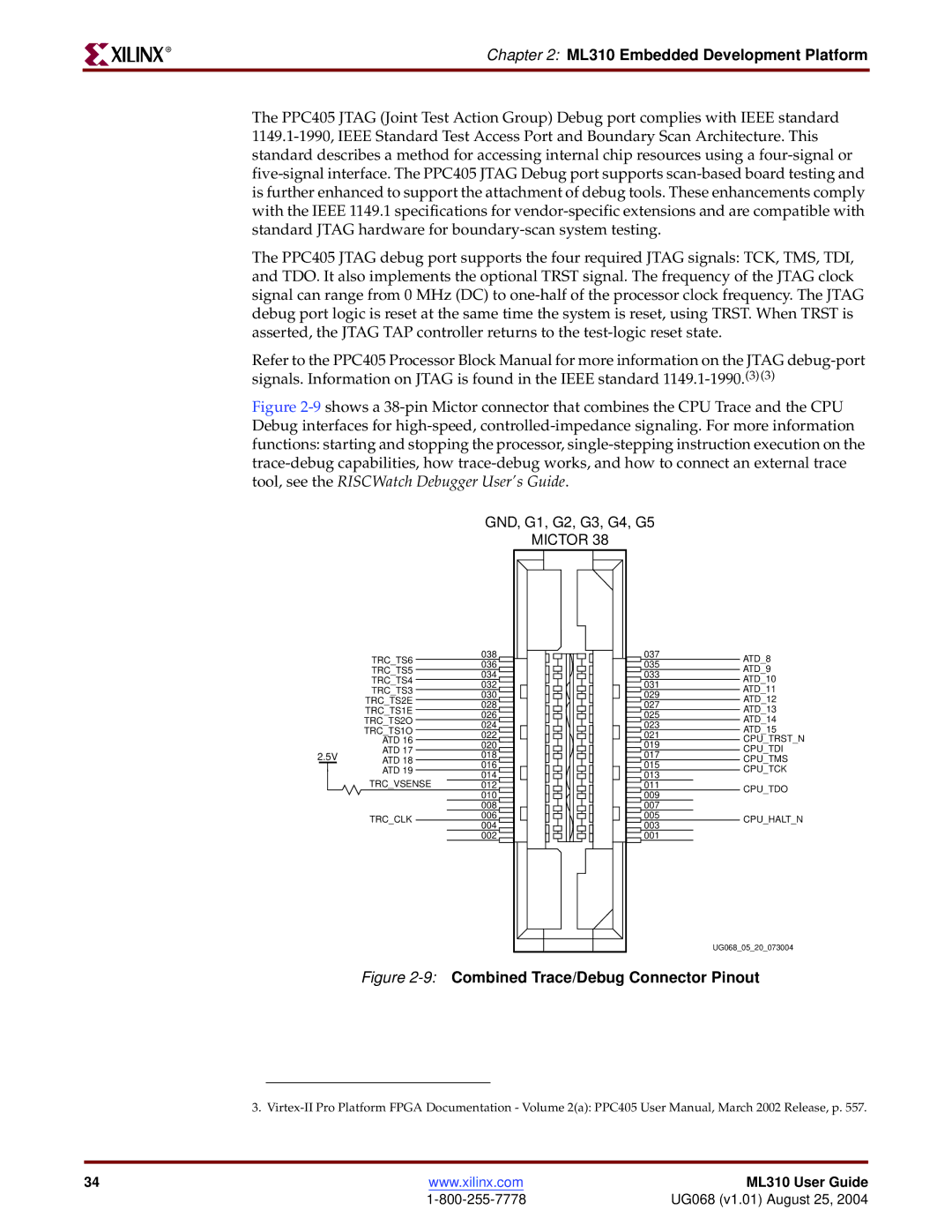
Figure 2-9 shows a 38-pin Mictor connector that combines the CPU Trace and the CPU Debug interfaces for high-speed, controlled-impedance signaling. For more information functions: starting and stopping the processor, single-stepping instruction execution on the trace-debug capabilities, how trace-debug works, and how to connect an external trace tool, see the RISCWatch Debugger User’s Guide.
|
| GND, G1, G2, G3, G4, G5 |
| ||
|
|
| MICTOR 38 |
| |
| TRC_TS6 | 038 | 037 | ATD_8 | |
| 036 | 035 | |||
| TRC_TS5 | ATD_9 | |||
| 034 | 033 | |||
| TRC_TS4 | ATD_10 | |||
| 032 | 031 | |||
| TRC_TS3 | ATD_11 | |||
| 030 | 029 | |||
| TRC_TS2E | ATD_12 | |||
| 028 | 027 | |||
| TRC_TS1E | ATD_13 | |||
| 026 | 025 | |||
| TRC_TS2O | ATD_14 | |||
| 024 | 023 | |||
| TRC_TS1O | ATD_15 | |||
| 022 | 021 | |||
| ATD 16 | CPU_TRST_N | |||
| 020 | 019 | |||
| ATD 17 | CPU_TDI | |||
2.5V | 018 | 017 | |||
ATD 18 | CPU_TMS | ||||
016 | 015 | ||||
| ATD 19 | CPU_TCK | |||
| 014 | 013 | |||
| TRC_VSENSE |
| |||
| 012 | 011 | CPU_TDO | ||
|
| 010 | 009 | ||
|
|
| |||
|
| 008 | 007 |
| |
| TRC_CLK | 006 | 005 | CPU_HALT_N | |
| 004 | 003 | |||
|
|
| |||
|
| 002 | 001 |
| |
|
|
|
| UG068_05_20_073004 | |
Figure 2-9: Combined Trace/Debug Connector Pinout
3.
34 | www.xilinx.com | ML310 User Guide |
| UG068 (v1.01) August 25, 2004 |
