Board Hardware
R
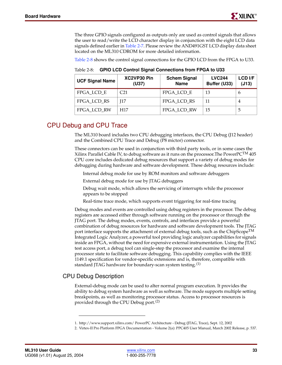
The three GPIO signals configured as outputs only are used as control signals that allows the user to read/write the LCD character display in conjunction with the eight LCD data signals defined earlier in Table
Table
Table
UCF Signal Name | XC2VP30 Pin | Schem Signal | LVC244 | LCD I/F | |
(U37) | Name | Buffer (U33) | (J13) | ||
| |||||
|
|
|
|
| |
FPGA_LCD_E | C21 | FPGA_LCD_E | 13 | 6 | |
|
|
|
|
| |
FPGA_LCD_RS | J17 | FPGA_LCD_RS | 11 | 4 | |
|
|
|
|
| |
FPGA_LCD_RW | H17 | FPGA_LCD_RW | 15 | 5 | |
|
|
|
|
|
CPU Debug and CPU Trace
The ML310 board includes two CPU debugging interfaces, the CPU Debug (J12 header) and the Combined CPU Trace and Debug (P8 mictor) connector.
These connectors can be used in conjunction with third party tools, or in some cases the Xilinx Parallel Cable IV, to debug software as it runs on the processor.The PowerPCTM 405 CPU core includes dedicated debug resources that support a variety of debug modes for debugging during hardware and software development. These debug resources include:
•Internal debug mode for use by ROM monitors and software debuggers
•External debug mode for use by JTAG debuggers
•Debug wait mode, which allows the servicing of interrupts while the processor appears to be stopped
•
Debug modes and events are controlled using debug registers in the processor. The debug registers are accessed either through software running on the processor or through the JTAG port. The debug modes, events, controls, and interfaces provide a powerful combination of debug resources for hardware and software development tools. The JTAG port interface supports the attachment of external debug tools, such as the ChipScopeTM Integrated Logic Analyzer, a powerful tool providing logic analyzer capabilities for signals inside an FPGA, without the need for expensive external instrumentation. Using the JTAG test access port, a debug tool can
CPU Debug Description
1.http://www.support.xilinx.com/ PowerPC Architecture - Debug (JTAG, Trace), Sept. 12, 2002
2.
ML310 User Guide | www.xilinx.com | 33 |
UG068 (v1.01) August 25, 2004 |
|