Board Hardware
R
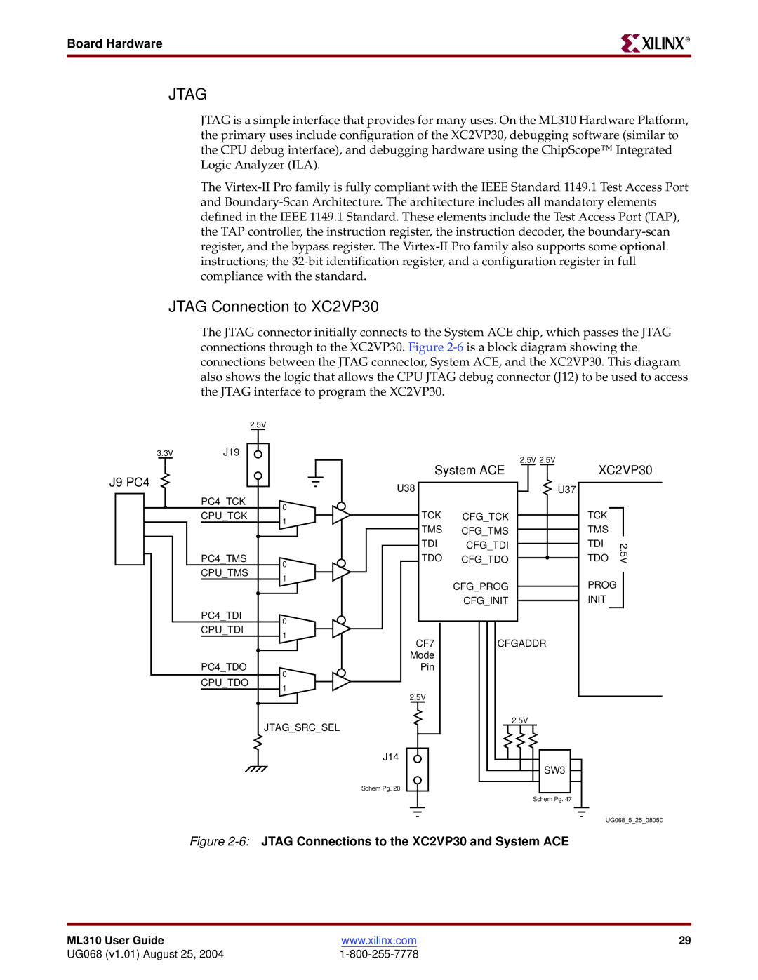
JTAG
JTAG is a simple interface that provides for many uses. On the ML310 Hardware Platform, the primary uses include configuration of the XC2VP30, debugging software (similar to the CPU debug interface), and debugging hardware using the ChipScope™ Integrated Logic Analyzer (ILA).
The
JTAG Connection to XC2VP30
The JTAG connector initially connects to the System ACE chip, which passes the JTAG connections through to the XC2VP30. Figure
|
|
|
|
|
|
|
| 2.5V |
|
| |||||||
|
|
|
|
|
|
|
|
|
|
|
|
|
|
|
|
|
|
|
| 3.3V | J19 |
|
|
|
|
|
|
|
|
|
| 2.5V 2.5V | |||
|
|
|
|
|
|
|
|
|
|
|
|
|
|
|
|
| |
J9 PC4 |
|
|
|
|
|
|
|
|
| System ACE | |||||||
|
|
|
|
|
|
|
|
|
|
|
| ||||||
|
|
|
|
|
|
|
| U38 |
| U37 | |||||||
|
|
|
|
|
| PC4_TCK | 0 |
|
|
|
|
| |||||
|
|
|
|
|
|
|
|
|
|
|
|
|
| ||||
|
|
|
|
|
| CPU_TCK |
|
|
|
|
| TCK | CFG_TCK | ||||
|
|
|
|
|
| 1 |
|
|
|
|
| ||||||
|
|
|
|
|
|
|
|
|
|
|
|
| TMS | CFG_TMS | |||
|
|
|
|
|
|
|
|
|
|
|
|
|
|
| |||
|
|
|
|
|
|
|
|
|
|
|
|
|
|
| TDI | CFG_TDI | |
|
|
|
|
|
| PC4_TMS | 0 |
|
|
|
|
| TDO | CFG_TDO | |||
|
|
|
|
|
| CPU_TMS |
|
|
|
|
|
|
|
| |||
|
|
|
|
|
| 1 |
|
|
|
|
|
|
|
| |||
|
|
|
|
|
|
|
|
|
|
|
|
|
| CFG_PROG | |||
|
|
|
|
|
|
|
|
|
|
|
|
|
|
|
| ||
|
|
|
|
|
|
|
|
|
|
|
|
|
|
|
| CFG_INIT | |
PC4_TDI | 0 |
|
CPU_TDI |
| |
1 |
| |
| CFGADDR | |
| CF7 | |
| Mode |
|
PC4_TDO | Pin |
|
CPU_TDO | 0 |
|
1 |
| |
|
| |
| 2.5V |
|
| JTAG_SRC_SEL | 2.5V |
|
| |
| J14 |
|
|
| SW3 |
| Schem Pg. 20 |
|
|
| Schem Pg. 47 |
Figure 2-6: JTAG Connections to the XC2VP30 and System ACE
XC2VP30
TCK |
|
TMS |
|
TDI | 2 |
TDO | .5V |
PROG
INIT
UG068_5_25_08050
ML310 User Guide | www.xilinx.com | 29 |
UG068 (v1.01) August 25, 2004 |
|