Board Hardware
R
CPU Debug Connector Pinout
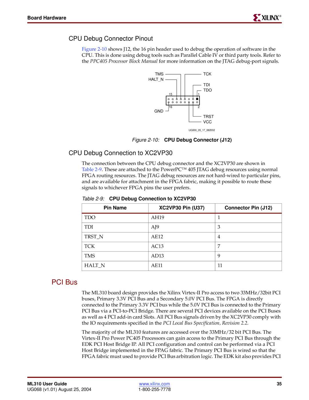
Figure 2-10 shows J12, the 16 pin header used to debug the operation of software in the CPU. This is done using debug tools such as Parallel Cable IV or third party tools. Refer to the PPC405 Processor Block Manual for more information on the JTAG debug-port signals.
TMS
HALT_N
15
16
GND
TCK
TDI
TDO
1
2
TRST
VCC
UG000_05_17_082002
Figure 2-10: CPU Debug Connector (J12)
CPU Debug Connection to XC2VP30
The connection between the CPU debug connector and the XC2VP30 are shown in Table
Table
Pin Name | XC2VP30 Pin (U37) | Connector Pin (J12) |
|
|
|
TDO | AH19 | 1 |
|
|
|
TDI | AJ9 | 3 |
|
|
|
TRST_N | AE12 | 4 |
|
|
|
TCK | AC13 | 7 |
|
|
|
TMS | AD13 | 9 |
|
|
|
HALT_N | AE11 | 11 |
|
|
|
PCI Bus
The ML310 board design provides the Xilinx
The majority of the ML310 features are accessed over the 33MHz/32 bit PCI Bus. The
ML310 User Guide | www.xilinx.com | 35 |
UG068 (v1.01) August 25, 2004 |
|