R
Chapter 2: ML310 Embedded Development Platform
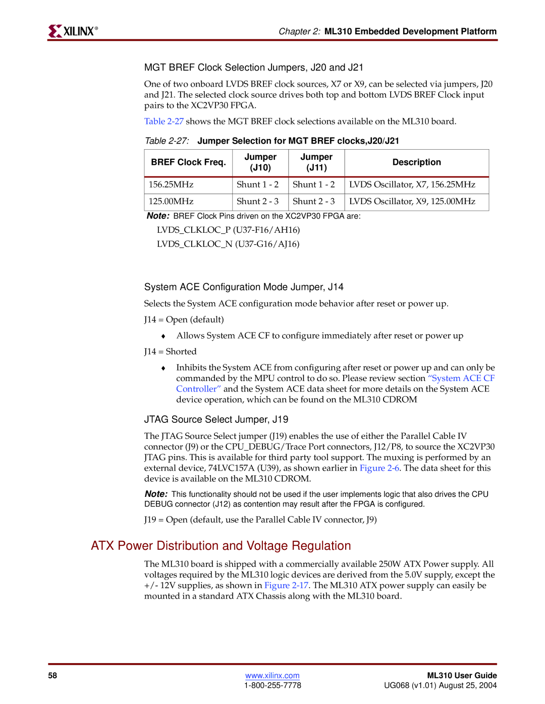
MGT BREF Clock Selection Jumpers, J20 and J21
One of two onboard LVDS BREF clock sources, X7 or X9, can be selected via jumpers, J20 and J21. The selected clock source drives both top and bottom LVDS BREF Clock input pairs to the XC2VP30 FPGA.
Table
Table
BREF Clock Freq. | Jumper | Jumper | Description | |
(J10) | (J11) | |||
|
| |||
|
|
|
| |
156.25MHz | Shunt 1 - 2 | Shunt 1 - 2 | LVDS Oscillator, X7, 156.25MHz | |
|
|
|
| |
125.00MHz | Shunt 2 - 3 | Shunt 2 - 3 | LVDS Oscillator, X9, 125.00MHz | |
|
|
|
|
Note: BREF Clock Pins driven on the XC2VP30 FPGA are:
LVDS_CLKLOC_P
LVDS_CLKLOC_N
System ACE Configuration Mode Jumper, J14
Selects the System ACE configuration mode behavior after reset or power up.
J14 = Open (default)
♦Allows System ACE CF to configure immediately after reset or power up J14 = Shorted
♦Inhibits the System ACE from configuring after reset or power up and can only be commanded by the MPU control to do so. Please review section “System ACE CF Controller” and the System ACE data sheet for more details on the System ACE device operation, which can be found on the ML310 CDROM
JTAG Source Select Jumper, J19
The JTAG Source Select jumper (J19) enables the use of either the Parallel Cable IV connector (J9) or the CPU_DEBUG/Trace Port connectors, J12/P8, to source the XC2VP30 JTAG pins. This is available for third party tool support. The muxing is performed by an external device, 74LVC157A (U39), as shown earlier in Figure
Note: This functionality should not be used if the user implements logic that also drives the CPU DEBUG connector (J12) as contention may result after the FPGA is configured.
J19 = Open (default, use the Parallel Cable IV connector, J9)
ATX Power Distribution and Voltage Regulation
The ML310 board is shipped with a commercially available 250W ATX Power supply. All voltages required by the ML310 logic devices are derived from the 5.0V supply, except the +/- 12V supplies, as shown in Figure
58 | www.xilinx.com | ML310 User Guide |
| UG068 (v1.01) August 25, 2004 |