R
Chapter 2: ML310 Embedded Development Platform
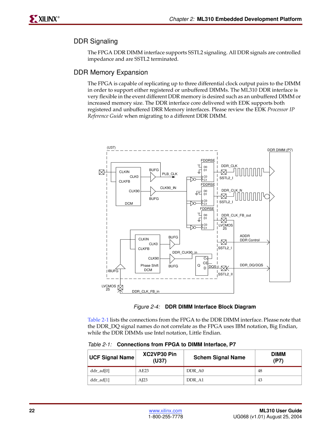
DDR Signaling
The FPGA DDR DIMM interface supports SSTL2 signaling. All DDR signals are controlled impedance and are SSTL2 terminated.
DDR Memory Expansion
The FPGA is capable of replicating up to three differential clock output pairs to the DIMM in order to support either registered or unbuffered DIMMs. The ML310 DDR interface is very flexible in the event different DDR memory is desired such as an unbuffered DIMM or increased memory size. The DDR interface core delivered with EDK supports both registered and unbuffered DRR Memory interfaces. Please review the EDK Processor IP Reference Guide when migrating to a different DDR DIMM.
(U37) |
|
|
|
|
|
| DDR DIMM (P7) |
|
|
|
|
|
|
| |
|
|
|
|
| FDDRSE |
| |
|
| BUFG |
|
| D0 | DDR_CLK |
|
| CLKIN |
|
| D1 |
|
| |
|
| PLB_CLK |
|
|
|
| |
| CLK0 |
| C0 |
|
| ||
|
|
| SSTL2_I |
| |||
| CLKFB |
|
|
| C1 |
| |
|
|
|
|
|
| ||
|
|
|
| FDDRSE |
| ||
|
|
| CLK90_IN |
|
| ||
| CLK90 |
| D0 | DDR_CLK_N | |||
|
|
| |||||
|
|
|
|
| D1 |
|
|
|
| BUFG |
|
| C0 | SSTL2_I |
|
| DCM |
|
|
|
| ||
|
|
|
| C1 |
| ||
|
|
|
|
|
| ||
|
|
|
| FDDRSE |
| ||
|
|
|
|
| D0 | DDR_CLK_FB_out | |
|
|
|
|
| D1 |
|
|
|
|
|
|
| C0 | LVCMOS |
|
|
|
|
|
| C1 | 25 |
|
|
| CLKIN | BUFG |
|
|
| ADDR |
|
|
|
|
| DDR Control | ||
|
|
|
|
|
| ||
|
| CLK0 |
|
|
|
|
|
|
| CLKFB | DDR_CLK90_in |
|
| SSTL2_I |
|
|
|
|
|
|
|
| |
|
| CLK90 |
|
| C |
|
|
|
| Phase Shift | BUFG | Q | CE | DQS_i | DDR_DQ/DQS |
IBUFG |
| DCM |
| D |
| ||
|
|
|
|
|
| ||
|
|
|
|
| SSTL2_II |
| |
|
|
|
|
|
|
| |
LVCMOS
25
DDR_CLK_FB_in
Figure 2-4: DDR DIMM Interface Block Diagram
Table
Table
UCF Signal Name | XC2VP30 Pin | Schem Signal Name | DIMM | |
(U37) | (P7) | |||
|
| |||
|
|
|
| |
ddr_ad[0] | AE23 | DDR_A0 | 48 | |
|
|
|
| |
ddr_ad[1] | AJ23 | DDR_A1 | 43 | |
|
|
|
|
22 | www.xilinx.com | ML310 User Guide |
| UG068 (v1.01) August 25, 2004 |