R
Chapter 2: ML310 Embedded Development Platform
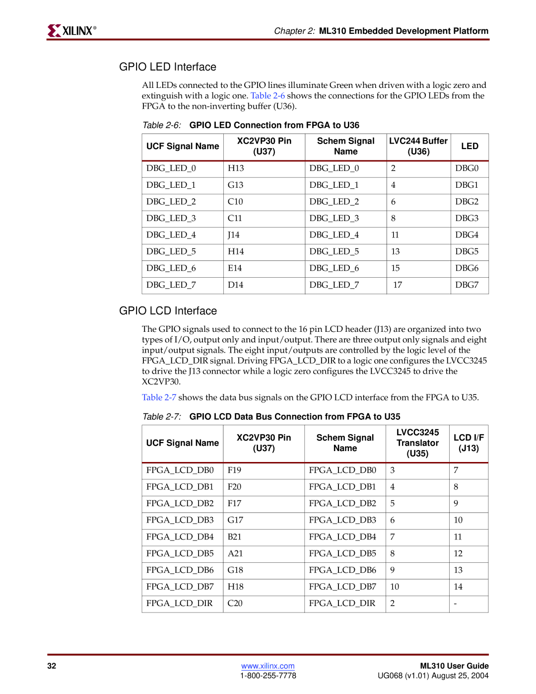
GPIO LED Interface
All LEDs connected to the GPIO lines illuminate Green when driven with a logic zero and extinguish with a logic one. Table
Table
UCF Signal Name | XC2VP30 Pin | Schem Signal | LVC244 Buffer | LED | |
(U37) | Name | (U36) | |||
|
| ||||
|
|
|
|
| |
DBG_LED_0 | H13 | DBG_LED_0 | 2 | DBG0 | |
|
|
|
|
| |
DBG_LED_1 | G13 | DBG_LED_1 | 4 | DBG1 | |
|
|
|
|
| |
DBG_LED_2 | C10 | DBG_LED_2 | 6 | DBG2 | |
|
|
|
|
| |
DBG_LED_3 | C11 | DBG_LED_3 | 8 | DBG3 | |
|
|
|
|
| |
DBG_LED_4 | J14 | DBG_LED_4 | 11 | DBG4 | |
|
|
|
|
| |
DBG_LED_5 | H14 | DBG_LED_5 | 13 | DBG5 | |
|
|
|
|
| |
DBG_LED_6 | E14 | DBG_LED_6 | 15 | DBG6 | |
|
|
|
|
| |
DBG_LED_7 | D14 | DBG_LED_7 | 17 | DBG7 | |
|
|
|
|
|
GPIO LCD Interface
The GPIO signals used to connect to the 16 pin LCD header (J13) are organized into two types of I/O, output only and input/output. There are three output only signals and eight input/output signals. The eight input/outputs are controlled by the logic level of the FPGA_LCD_DIR signal. Driving FPGA_LCD_DIR to a logic one configures the LVCC3245 to drive the J13 connector while a logic zero configures the LVCC3245 to drive the XC2VP30.
Table
Table
| XC2VP30 Pin | Schem Signal |
| LVCC3245 | LCD I/F |
UCF Signal Name |
| Translator | |||
(U37) | Name |
| (J13) | ||
|
| (U35) | |||
|
|
|
|
| |
|
|
|
|
|
|
FPGA_LCD_DB0 | F19 | FPGA_LCD_DB0 | 3 |
| 7 |
|
|
|
|
|
|
FPGA_LCD_DB1 | F20 | FPGA_LCD_DB1 | 4 |
| 8 |
|
|
|
|
|
|
FPGA_LCD_DB2 | F17 | FPGA_LCD_DB2 | 5 |
| 9 |
|
|
|
|
|
|
FPGA_LCD_DB3 | G17 | FPGA_LCD_DB3 | 6 |
| 10 |
|
|
|
|
|
|
FPGA_LCD_DB4 | B21 | FPGA_LCD_DB4 | 7 |
| 11 |
|
|
|
|
|
|
FPGA_LCD_DB5 | A21 | FPGA_LCD_DB5 | 8 |
| 12 |
|
|
|
|
|
|
FPGA_LCD_DB6 | G18 | FPGA_LCD_DB6 | 9 |
| 13 |
|
|
|
|
| |
FPGA_LCD_DB7 | H18 | FPGA_LCD_DB7 | 10 | 14 | |
|
|
|
|
|
|
FPGA_LCD_DIR | C20 | FPGA_LCD_DIR | 2 |
| - |
|
|
|
|
|
|
32 | www.xilinx.com | ML310 User Guide |
| UG068 (v1.01) August 25, 2004 |