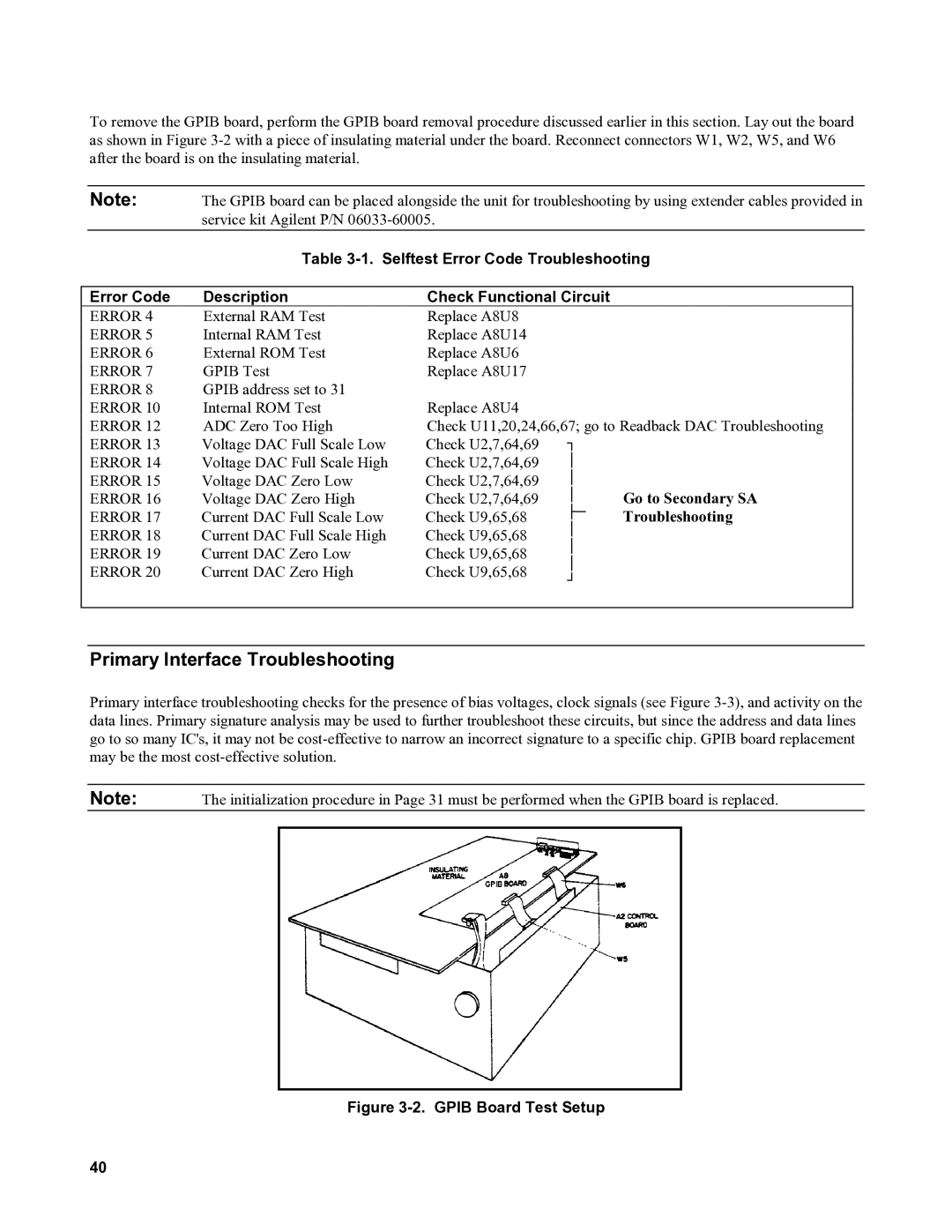
To remove the GPIB board, perform the GPIB board removal procedure discussed earlier in this section. Lay out the board as shown in Figure
Note: The GPIB board can be placed alongside the unit for troubleshooting by using extender cables provided in service kit Agilent P/N
Table
Error Code | Description | Check Functional Circuit |
| ||
ERROR 4 | External RAM Test | Replace A8U8 |
|
| |
ERROR 5 | Internal RAM Test | Replace A8U14 |
|
| |
ERROR 6 | External ROM Test | Replace A8U6 |
|
| |
ERROR 7 | GPIB Test | Replace A8U17 |
|
| |
ERROR 8 | GPIB address set to 31 |
|
|
| |
ERROR 10 | Internal ROM Test | Replace A8U4 |
|
| |
ERROR 12 | ADC Zero Too High | Check U11,20,24,66,67; go to Readback DAC Troubleshooting | |||
ERROR 13 | Voltage DAC Full Scale Low | Check U2,7,64,69 | ┐ |
| |
ERROR 14 | Voltage DAC Full Scale High | Check U2,7,64,69 | │ |
| |
ERROR 15 | Voltage DAC Zero Low | Check U2,7,64,69 | │ |
| |
ERROR 16 | Voltage DAC Zero High | Check U2,7,64,69 | │ | Go to Secondary SA | |
ERROR 17 | Current DAC Full Scale Low | Check U9,65,68 | ├─ | Troubleshooting | |
│ | |||||
ERROR 18 | Current DAC Full Scale High | Check U9,65,68 |
| ||
│ |
| ||||
ERROR 19 | Current DAC Zero Low | Check U9,65,68 |
| ||
│ |
| ||||
ERROR 20 | Current DAC Zero High | Check U9,65,68 |
| ||
┘ |
| ||||
|
|
|
| ||
|
|
|
|
| |
Primary Interface Troubleshooting
Primary interface troubleshooting checks for the presence of bias voltages, clock signals (see Figure
Note: The initialization procedure in Page 31 must be performed when the GPIB board is replaced.
Figure 3-2. GPIB Board Test Setup
40