ADSP-TS201S
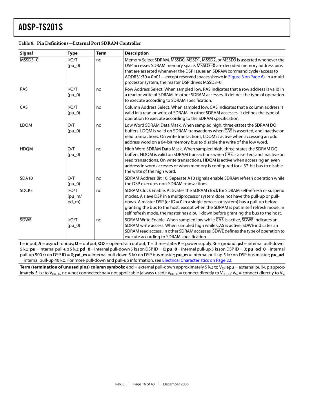
Table 8. Pin Definitions—External Port SDRAM Controller
| Signal |
| Type | Term | Description | |||||||||||||||||||||||||||||||||
|
|
|
|
|
| I/O/T | nc | Memory Select SDRAM. |
|
|
|
|
|
|
|
|
|
|
|
|
|
| or |
|
|
|
|
|
|
|
| is asserted whenever the | ||||||
| MSSD0, | MSSD1, | MSSD2, | MSSD3 | ||||||||||||||||||||||||||||||||||
|
|
|
|
|
| (pu_0) |
| DSP accesses SDRAM memory space. |
| are decoded memory address pins | ||||||||||||||||||||||||||||
|
|
|
|
|
|
|
| that are asserted whenever the DSP issues an SDRAM command cycle (access to | ||||||||||||||||||||||||||||||
|
|
|
|
|
|
|
| ADDR31:30 = | ||||||||||||||||||||||||||||||
|
|
|
|
|
|
|
| processor system, the master DSP drives |
|
|
|
|
|
|
|
|
|
|
|
|
|
|
|
|
|
|
| |||||||||||
|
|
|
|
|
|
|
| |||||||||||||||||||||||||||||||
|
|
|
|
|
| I/O/T | nc | Row Address Select. When sampled low, |
|
| indicates that a row address is valid in | |||||||||||||||||||||||||||
| RAS | RAS | ||||||||||||||||||||||||||||||||||||
|
|
|
|
|
| (pu_0) |
| a read or write of SDRAM. In other SDRAM accesses, it defines the type of operation | ||||||||||||||||||||||||||||||
|
|
|
|
|
|
|
| to execute according to SDRAM specification. | ||||||||||||||||||||||||||||||
|
|
|
|
| I/O/T | nc | Column Address Select. When sampled low, |
|
|
|
| indicates that a column address is | ||||||||||||||||||||||||||
CAS | CAS | |||||||||||||||||||||||||||||||||||||
|
|
|
|
|
| (pu_0) |
| valid in a read or write of SDRAM. In other SDRAM accesses, it defines the type of | ||||||||||||||||||||||||||||||
|
|
|
|
|
|
|
| operation to execute according to the SDRAM specification. | ||||||||||||||||||||||||||||||
| LDQM |
| O/T | nc | Low Word SDRAM Data Mask. When sampled high, | |||||||||||||||||||||||||||||||||
|
|
|
|
|
| (pu_0) |
| buffers. LDQM is valid on SDRAM transactions when |
|
|
| is asserted, and inactive on | ||||||||||||||||||||||||||
|
|
|
|
|
| CAS | ||||||||||||||||||||||||||||||||
|
|
|
|
|
|
|
| read transactions. On write transactions, LDQM is active when accessing an odd | ||||||||||||||||||||||||||||||
|
|
|
|
|
|
|
| address word on a | ||||||||||||||||||||||||||||||
HDQM |
| O/T | nc | High Word SDRAM Data Mask. When sampled high, | ||||||||||||||||||||||||||||||||||
|
|
|
|
|
| (pu_0) |
| buffers. HDQM is valid on SDRAM transactions when |
| is asserted, and inactive on | ||||||||||||||||||||||||||||
|
|
|
|
|
| CAS | ||||||||||||||||||||||||||||||||
|
|
|
|
|
|
|
| read transactions. On write transactions, HDQM is active when accessing an even | ||||||||||||||||||||||||||||||
|
|
|
|
|
|
|
| address in word accesses or when memory is configured for a | ||||||||||||||||||||||||||||||
|
|
|
|
|
|
|
| the write of the high word. | ||||||||||||||||||||||||||||||
| SDA10 |
| O/T | nc | SDRAM Address Bit 10. Separate A10 signals enable SDRAM refresh operation while | |||||||||||||||||||||||||||||||||
|
|
|
|
|
| (pu_0) |
| the DSP executes | ||||||||||||||||||||||||||||||
SDCKE |
| I/O/T | nc | SDRAM Clock Enable. Activates the SDRAM clock for SDRAM | ||||||||||||||||||||||||||||||||||
|
|
|
|
|
| (pu_m/ |
| modes. A slave DSP in a multiprocessor system does not have the | ||||||||||||||||||||||||||||||
|
|
|
|
|
| pd_m) |
| down. A master DSP (or ID = 0 in a single processor system) has a | ||||||||||||||||||||||||||||||
|
|
|
|
|
|
|
| granting the bus to the host, except when the SDRAM is put in self refresh mode. In | ||||||||||||||||||||||||||||||
|
|
|
|
|
|
|
| self refresh mode, the master has a | ||||||||||||||||||||||||||||||
|
|
|
| I/O/T | nc | SDRAM Write Enable. When sampled low while |
|
|
|
| is active, |
|
|
| indicates an | |||||||||||||||||||||||
SDWE | CAS | SDWE | ||||||||||||||||||||||||||||||||||||
|
|
|
|
|
| (pu_0) |
| SDRAM write access. When sampled high while | CAS | is active, | SDWE | indicates an | ||||||||||||||||||||||||||
|
|
|
|
|
|
|
| SDRAM read access. In other SDRAM accesses, | SDWE | defines the type of operation to | ||||||||||||||||||||||||||||
|
|
|
|
|
|
|
| execute according to SDRAM specification. | ||||||||||||||||||||||||||||||
I = input; A = asynchronous; O = output; OD =
5kΩ; pu = internal
Term (termination of unused pins) column symbols: epd = external
Rev. C Page 16 of 48 December 2006