|
|
|
|
|
|
|
|
|
| |
|
|
|
|
|
|
|
|
|
|
|
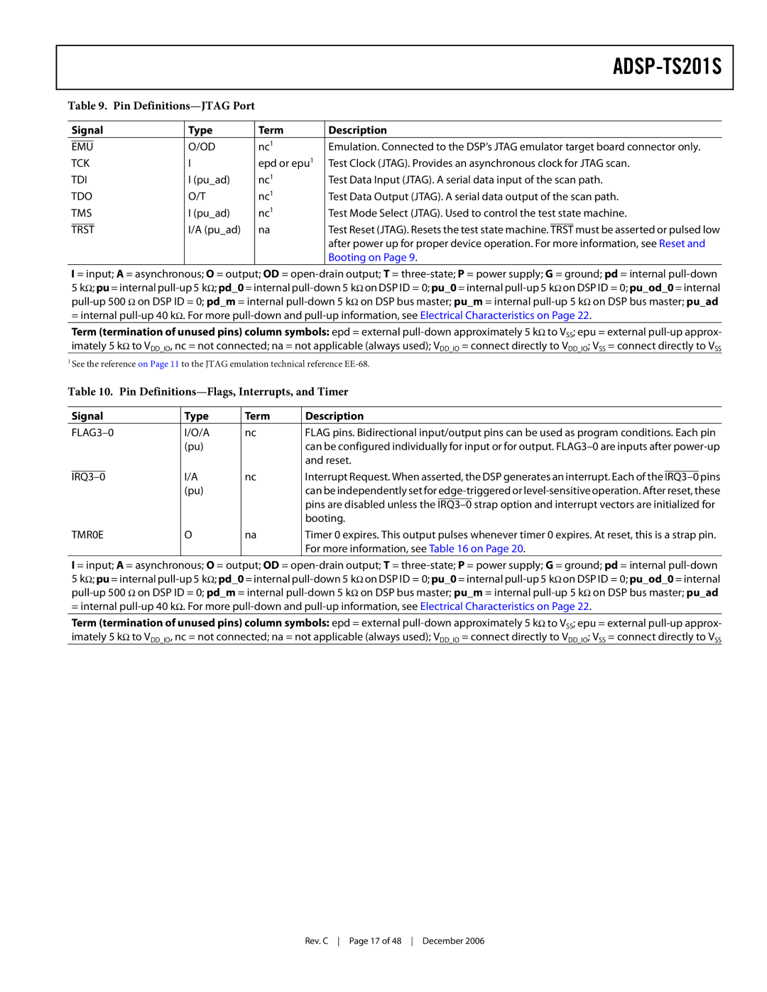
| Table 9. Pin |
|
|
|
|
| ||||
|
|
|
|
|
|
| ||||
|
| Signal | Type | Term | Description |
| ||||
|
|
|
|
| O/OD | nc1 | Emulation. Connected to the DSP’s JTAG emulator target board connector only. | |||
|
| EMU | ||||||||
|
| TCK | I | epd or epu1 | Test Clock (JTAG). Provides an asynchronous clock for JTAG scan. | |||||
|
| TDI | I (pu_ad) | nc1 | Test Data Input (JTAG). A serial data input of the scan path. | |||||
|
| TDO | O/T | nc1 | Test Data Output (JTAG). A serial data output of the scan path. | |||||
|
| TMS | I (pu_ad) | nc1 | Test Mode Select (JTAG). Used to control the test state machine. | |||||
|
|
|
| I/A (pu_ad) | na | Test Reset (JTAG). Resets the test state machine. |
| must be asserted or pulsed low | ||
|
| TRST | TRST | |||||||
|
|
|
|
|
|
| after power up for proper device operation. For more information, see Reset and | |||
|
|
|
|
|
|
| Booting on Page 9. |
| ||
I = input; A = asynchronous; O = output; OD =
5kΩ; pu = internal
Term (termination of unused pins) column symbols: epd = external
1See the reference on Page 11 to the JTAG emulation technical reference
Table 10. Pin Definitions—Flags, Interrupts, and Timer
| Signal | Type | Term | Description | |||||
|
| I/O/A | nc | FLAG pins. Bidirectional input/output pins can be used as program conditions. Each pin | |||||
|
|
| (pu) |
| can be configured individually for input or for output. | ||||
|
|
|
|
| and reset. | ||||
|
|
| I/A | nc | Interrupt Request. When asserted, the DSP generates an interrupt. Each of the |
| pins | ||
| |||||||||
|
|
| (pu) |
| can be independently set for | ||||
|
|
|
|
| pins are disabled unless the |
| strap option and interrupt vectors are initialized for | ||
|
|
|
|
| |||||
|
|
|
|
| booting. | ||||
| TMR0E | O | na | Timer 0 expires. This output pulses whenever timer 0 expires. At reset, this is a strap pin. | |||||
|
|
|
|
| For more information, see Table 16 on Page 20. | ||||
I = input; A = asynchronous; O = output; OD =
5kΩ; pu = internal
Term (termination of unused pins) column symbols: epd = external
Rev. C Page 17 of 48 December 2006