ADSP-TS201S
PIN FUNCTION DESCRIPTIONS
While most of the ADSP-TS201S processor’s input pins are nor- mally synchronous—tied to a specific clock—a few are asynchronous. For these asynchronous signals, an on-chip syn- chronization circuit prevents metastability problems. Use the ac specification for asynchronous signals when the system design requires predictable, cycle-by-cycle behavior for these signals.
Table 3. Pin Definitions—Clocks and Reset
The output pins can be three-stated during normal operation. The DSP three-states all output pins during reset, allowing these pins to get to their internal pull-up or pull-down state. Some pins have an internal pull-up or pull-down resistor (±30% toler- ance) that maintains a known value during transitions between different drivers.
| | | | | | | | | | | | | |
| Signal | Type | Term | Description |
| SCLKRAT2–0 | I (pd) | na | Core Clock Ratio. The DSP’s core clock (CCLK) rate = n × SCLK, where n is user- |
| | | | | | | programmable using the SCLKRATx pins to the values shown in Table 4. These pins |
| | | | | | | may change only during reset; connect these pins to VDD_IO or VSS. All reset specifica- |
| | | | | | | tions in Table 25, Table 26, and Table 27 must be satisfied. The core clock rate (CCLK) |
| | | | | | | is the instruction cycle rate. |
SCLK | I | na | System Clock Input. The DSP’s system input clock for cluster bus. The core clock rate |
| | | | | | | is user-programmable using the SCLKRATx pins. For more information, see Clock |
| | | | | | | |
| | | | | I/A | na | Reset. Sets the DSP to a known state and causes program to be in idle state. | | |
RST_IN | RST_IN |
| | | | | | | must be asserted a specified time according to the type of reset operation. For details, |
| | | | | | | see Reset and Booting on Page 9, Table 25 on Page 26, and Figure 13 on Page 26. |
| | | | O | na | Reset Output. Indicates that the DSP reset is complete. Connect to | | |
RST_OUT | POR_IN. |
| | | I/A | na | Power-On Reset for internal DRAM. Connect to | | |
| POR_IN | RST_OUT. |
I = input; A = asynchronous; O = output; OD = open-drain output; T = three-state; P = power supply; G = ground; pd = internal pull-down
5kΩ; pu = internal pull-up 5 kΩ; pd_0 = internal pull-down 5 kΩ on DSP ID = 0; pu_0 = internal pull-up 5 kΩ on DSP ID = 0; pu_od_0 = internal pull-up 500 Ω on DSP ID = 0; pd_m = internal pull-down 5 kΩ on DSP bus master; pu_m = internal pull-up 5 kΩ on DSP bus master; pu_ad = internal pull-up 40 kΩ. For more pull-down and pull-up information, see Electrical Characteristics on Page 22.
Term (termination of unused pins) column symbols: epd = external pull-down approximately 5 kΩ to VSS; epu = external pull-up approx- imately 5 kΩ to VDD_IO, nc = not connected; na = not applicable (always used); VDD_IO = connect directly to VDD_IO; VSS = connect directly to VSS
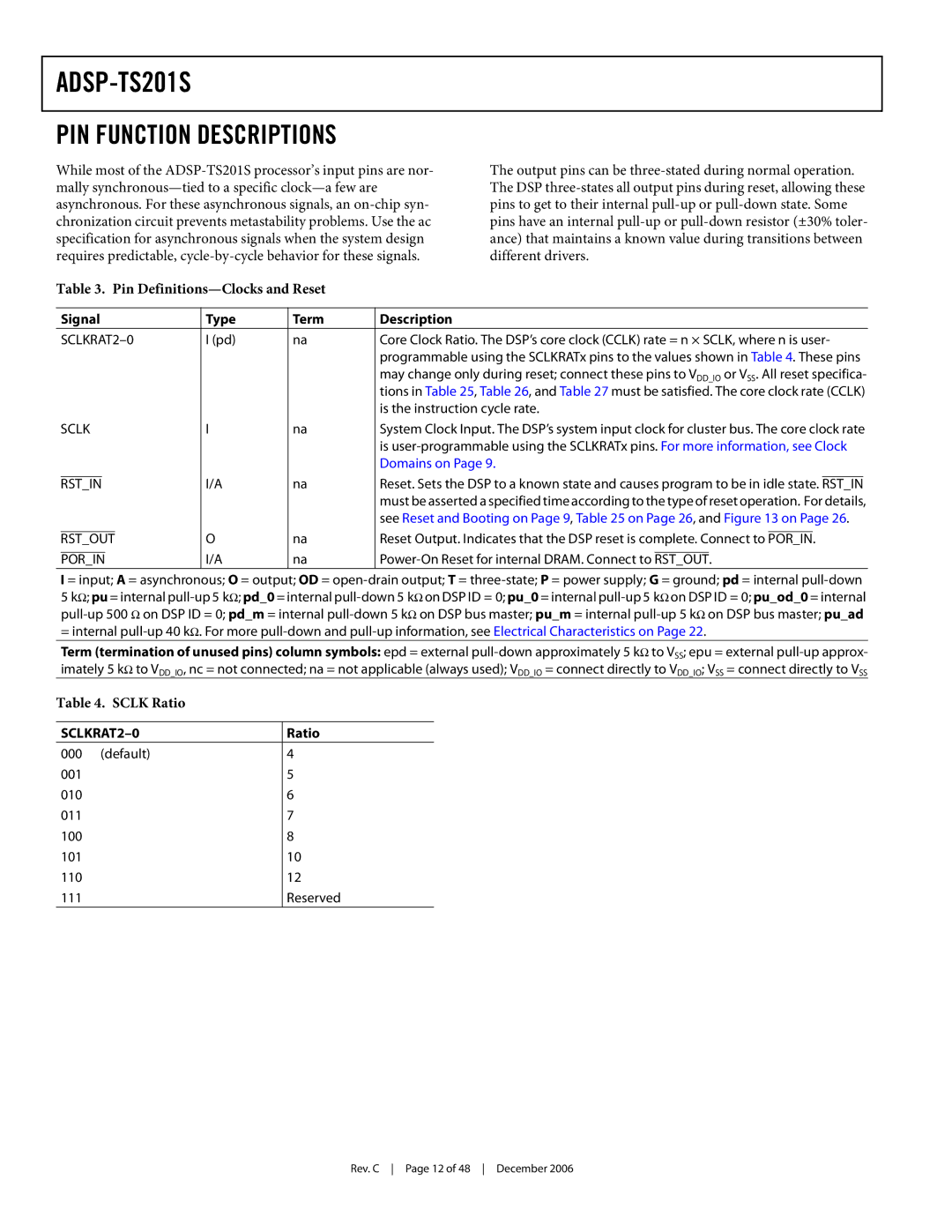
Table 4. SCLK Ratio
SCLKRAT2–0 | Ratio |
000 | (default) | 4 |
001 | | 5 |
010 | | 6 |
011 | | 7 |
100 | | 8 |
101 | | 10 |
110 | | 12 |
111 | | Reserved |
Rev. C Page 12 of 48 December 2006