|
|
|
|
|
|
|
|
|
|
|
|
|
|
|
|
|
|
|
|
|
|
|
|
|
|
|
|
|
|
|
|
|
|
|
|
|
|
|
|
|
|
|
|
|
|
|
|
|
|
|
|
|
|
|
|
|
|
| |||||||||
|
|
|
|
|
|
|
|
|
|
|
|
|
|
|
|
|
|
|
|
|
|
|
|
|
|
|
|
|
|
|
|
|
|
|
|
|
|
|
|
|
|
|
|
|
|
|
|
|
|
|
|
|
|
|
|
|
|
|
|
|
|
|
|
|
|
|
|
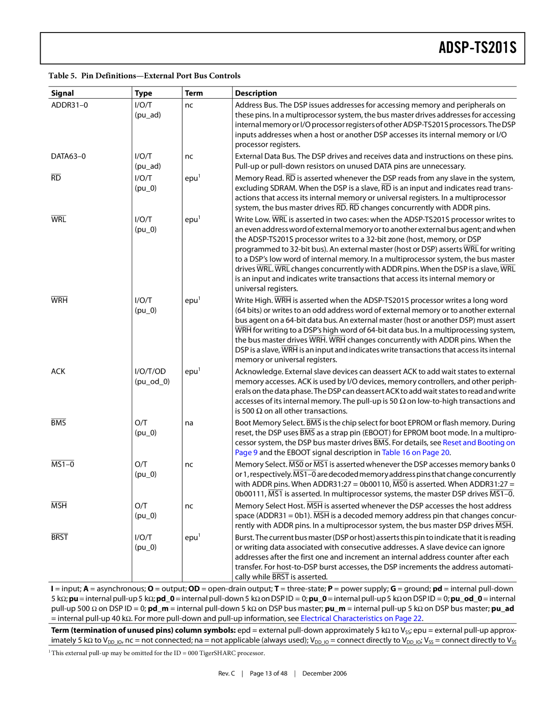
| Table 5. Pin | ||||||||||||||||||||||||||||||||||||||||||||||||||||||||||||||||||
|
|
|
|
|
|
|
| ||||||||||||||||||||||||||||||||||||||||||||||||||||||||||||
|
| Signal | Type | Term |
| Description |
| ||||||||||||||||||||||||||||||||||||||||||||||||||||||||||||
|
| I/O/T | nc | Address Bus. The DSP issues addresses for accessing memory and peripherals on | |||||||||||||||||||||||||||||||||||||||||||||||||||||||||||||||
|
|
|
|
|
|
|
|
|
| (pu_ad) |
| these pins. In a multiprocessor system, the bus master drives addresses for accessing | |||||||||||||||||||||||||||||||||||||||||||||||||||||||
|
|
|
|
|
|
|
|
|
|
|
| internal memory or I/O processor registers of other | |||||||||||||||||||||||||||||||||||||||||||||||||||||||
|
|
|
|
|
|
|
|
|
|
|
| inputs addresses when a host or another DSP accesses its internal memory or I/O | |||||||||||||||||||||||||||||||||||||||||||||||||||||||
|
|
|
|
|
|
|
|
|
|
|
| processor registers. | |||||||||||||||||||||||||||||||||||||||||||||||||||||||
| I/O/T | nc | External Data Bus. The DSP drives and receives data and instructions on these pins. | ||||||||||||||||||||||||||||||||||||||||||||||||||||||||||||||||
|
|
|
|
|
|
|
|
|
| (pu_ad) |
| ||||||||||||||||||||||||||||||||||||||||||||||||||||||||
|
|
|
|
|
|
|
|
|
| I/O/T | epu1 |
| Memory Read. |
|
|
|
|
|
|
| is asserted whenever the DSP reads from any slave in the system, | ||||||||||||||||||||||||||||||||||||||||||||||
RD | RD | ||||||||||||||||||||||||||||||||||||||||||||||||||||||||||||||||||
|
|
|
|
|
|
|
|
|
| (pu_0) |
|
| excluding SDRAM. When the DSP is a slave, | RD |
| is an input and indicates read trans- | |||||||||||||||||||||||||||||||||||||||||||||||||||
|
|
|
|
|
|
|
|
|
|
|
|
| actions that access its internal memory or universal registers. In a multiprocessor | ||||||||||||||||||||||||||||||||||||||||||||||||||||||
|
|
|
|
|
|
|
|
|
|
|
|
| system, the bus master drives |
|
|
|
| changes concurrently with ADDR pins. | |||||||||||||||||||||||||||||||||||||||||||||||||
|
|
|
|
|
|
|
|
|
|
|
| RD. | RD | ||||||||||||||||||||||||||||||||||||||||||||||||||||||
|
|
|
|
|
|
|
|
| I/O/T | epu1 |
| Write Low. |
|
|
|
|
|
| is asserted in two cases: when the | ||||||||||||||||||||||||||||||||||||||||||||||||
|
| WRL | WRL | ||||||||||||||||||||||||||||||||||||||||||||||||||||||||||||||||
|
|
|
|
|
|
|
|
|
| (pu_0) |
|
| an even address word of external memory or to another external bus agent; and when | ||||||||||||||||||||||||||||||||||||||||||||||||||||||
|
|
|
|
|
|
|
|
|
|
|
|
| the | ||||||||||||||||||||||||||||||||||||||||||||||||||||||
|
|
|
|
|
|
|
|
|
|
|
|
| programmed to | WRL | for writing | ||||||||||||||||||||||||||||||||||||||||||||||||||||
|
|
|
|
|
|
|
|
|
|
|
|
| to a DSP’s low word of internal memory. In a multiprocessor system, the bus master | ||||||||||||||||||||||||||||||||||||||||||||||||||||||
|
|
|
|
|
|
|
|
|
|
|
|
| drives |
|
|
|
|
|
|
|
|
|
|
| changes concurrently with ADDR pins. When the DSP is a slave, |
|
|
|
|
| |||||||||||||||||||||||||||||||||||||
|
|
|
|
|
|
|
|
|
|
|
| WRL. | WRL | WRL | |||||||||||||||||||||||||||||||||||||||||||||||||||||
|
|
|
|
|
|
|
|
|
|
|
|
| is an input and indicates write transactions that access its internal memory or | ||||||||||||||||||||||||||||||||||||||||||||||||||||||
|
|
|
|
|
|
|
|
|
|
|
|
| universal registers. | ||||||||||||||||||||||||||||||||||||||||||||||||||||||
|
|
|
|
|
|
|
| I/O/T | epu1 |
| Write High. |
|
|
|
|
| is asserted when the | ||||||||||||||||||||||||||||||||||||||||||||||||||
WRH | WRH | ||||||||||||||||||||||||||||||||||||||||||||||||||||||||||||||||||
|
|
|
|
|
|
|
|
|
| (pu_0) |
|
| (64 bits) or writes to an odd address word of external memory or to another external | ||||||||||||||||||||||||||||||||||||||||||||||||||||||
|
|
|
|
|
|
|
|
|
|
|
|
| bus agent on a | ||||||||||||||||||||||||||||||||||||||||||||||||||||||
|
|
|
|
|
|
|
|
|
|
|
|
|
| for writing to a DSP’s high word of | |||||||||||||||||||||||||||||||||||||||||||||||||||||
|
|
|
|
|
|
|
|
|
|
|
|
| WRH | ||||||||||||||||||||||||||||||||||||||||||||||||||||||
|
|
|
|
|
|
|
|
|
|
|
|
| the bus master drives | WRH. |
|
| WRH | changes concurrently with ADDR pins. When the | |||||||||||||||||||||||||||||||||||||||||||||||||
|
|
|
|
|
|
|
|
|
|
|
|
| DSP is a slave, | WRH | is an input and indicates write transactions that access its internal | ||||||||||||||||||||||||||||||||||||||||||||||||||||
|
|
|
|
|
|
|
|
|
|
|
|
| memory or universal registers. | ||||||||||||||||||||||||||||||||||||||||||||||||||||||
| ACK | I/O/T/OD | epu1 |
| Acknowledge. External slave devices can deassert ACK to add wait states to external | ||||||||||||||||||||||||||||||||||||||||||||||||||||||||||||||
|
|
|
|
|
|
|
|
|
| (pu_od_0) |
|
| memory accesses. ACK is used by I/O devices, memory controllers, and other periph- | ||||||||||||||||||||||||||||||||||||||||||||||||||||||
|
|
|
|
|
|
|
|
|
|
|
|
| erals on the data phase. The DSP can deassert ACK to add wait states to read and write | ||||||||||||||||||||||||||||||||||||||||||||||||||||||
|
|
|
|
|
|
|
|
|
|
|
|
| accesses of its internal memory. The | ||||||||||||||||||||||||||||||||||||||||||||||||||||||
|
|
|
|
|
|
|
|
|
|
|
|
| is 500 Ω on all other transactions. | ||||||||||||||||||||||||||||||||||||||||||||||||||||||
|
|
|
|
|
|
| O/T | na |
| Boot Memory Select. |
|
|
|
|
|
|
| is the chip select for boot EPROM or flash memory. During | |||||||||||||||||||||||||||||||||||||||||||||||||
|
| BMS |
| BMS | |||||||||||||||||||||||||||||||||||||||||||||||||||||||||||||||
|
|
|
|
|
|
|
|
|
| (pu_0) |
|
| reset, the DSP uses | BMS |
| as a strap pin (EBOOT) for EPROM boot mode. In a multipro- | |||||||||||||||||||||||||||||||||||||||||||||||||||
|
|
|
|
|
|
|
|
|
|
|
|
| cessor system, the DSP bus master drives | BMS. | For details, see Reset and Booting on | ||||||||||||||||||||||||||||||||||||||||||||||||||||
|
|
|
|
|
|
|
|
|
|
|
|
| Page 9 and the EBOOT signal description in Table 16 on Page 20. | ||||||||||||||||||||||||||||||||||||||||||||||||||||||
|
|
|
|
|
| O/T | nc |
| Memory Select. |
|
|
| or |
|
|
|
| is asserted whenever the DSP accesses memory banks 0 | |||||||||||||||||||||||||||||||||||||||||||||||||
|
|
| MS0 | MS1 | |||||||||||||||||||||||||||||||||||||||||||||||||||||||||||||||
|
|
|
|
|
|
|
|
|
| (pu_0) |
|
| or 1, respectively. | are decoded memory address pins that change concurrently | |||||||||||||||||||||||||||||||||||||||||||||||||||||
|
|
|
|
|
|
|
|
|
|
|
|
| with ADDR pins. When ADDR31:27 = 0b00110, | MS0 | is asserted. When ADDR31:27 = | ||||||||||||||||||||||||||||||||||||||||||||||||||||
|
|
|
|
|
|
|
|
|
|
|
|
| 0b00111, | MS1 | is asserted. In multiprocessor systems, the master DSP drives |
|
| ||||||||||||||||||||||||||||||||||||||||||||||||||
|
|
|
|
| O/T | nc | Memory Select Host. |
|
| is asserted whenever the DSP accesses the host address | |||||||||||||||||||||||||||||||||||||||||||||||||||||||||
|
| MSH | MSH | ||||||||||||||||||||||||||||||||||||||||||||||||||||||||||||||||
|
|
|
|
|
|
|
|
|
| (pu_0) |
|
| space (ADDR31 = 0b1). | MSH | is a decoded memory address pin that changes concur- | ||||||||||||||||||||||||||||||||||||||||||||||||||||
|
|
|
|
|
|
|
|
|
|
|
|
| rently with ADDR pins. In a multiprocessor system, the bus master DSP drives | MSH. |
|
| |||||||||||||||||||||||||||||||||||||||||||||||||||
|
|
|
| I/O/T | epu1 |
| Burst. The current bus master (DSP or host) asserts this pin to indicate that it is reading | ||||||||||||||||||||||||||||||||||||||||||||||||||||||||||||
|
| BRST |
| ||||||||||||||||||||||||||||||||||||||||||||||||||||||||||||||||
|
|
|
|
|
|
|
|
|
| (pu_0) |
|
| or writing data associated with consecutive addresses. A slave device can ignore | ||||||||||||||||||||||||||||||||||||||||||||||||||||||
|
|
|
|
|
|
|
|
|
|
|
|
| addresses after the first one and increment an internal address counter after each | ||||||||||||||||||||||||||||||||||||||||||||||||||||||
|
|
|
|
|
|
|
|
|
|
|
|
| transfer. For | ||||||||||||||||||||||||||||||||||||||||||||||||||||||
|
|
|
|
|
|
|
|
|
|
|
|
| cally while |
| is asserted. |
| |||||||||||||||||||||||||||||||||||||||||||||||||||
|
|
|
|
|
|
|
|
|
|
|
|
| BRST | ||||||||||||||||||||||||||||||||||||||||||||||||||||||
I = input; A = asynchronous; O = output; OD =
5kΩ; pu = internal
Term (termination of unused pins) column symbols: epd = external
1This external
Rev. C Page 13 of 48 December 2006