ADSP-TS201S
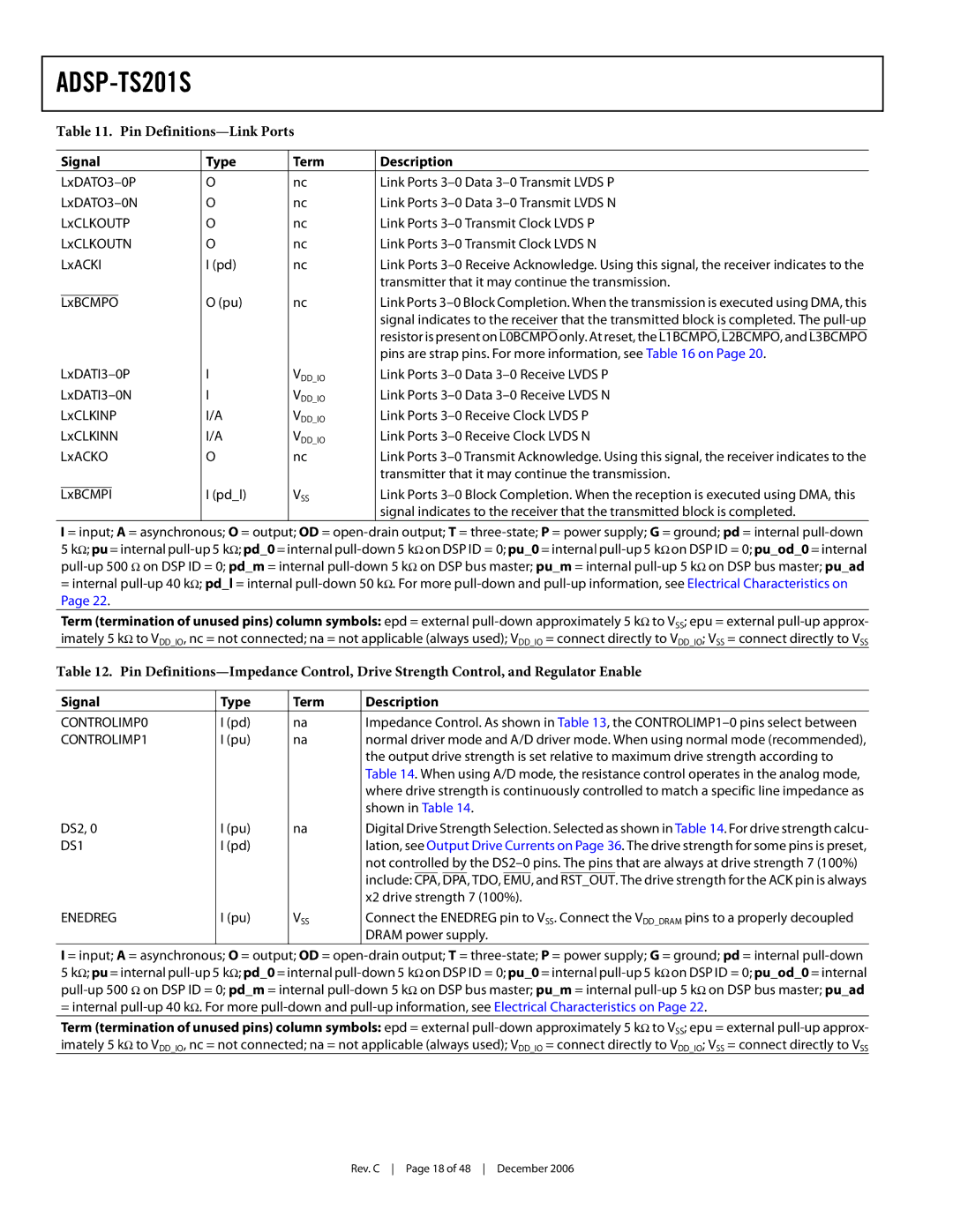
Table 11. Pin Definitions—Link Ports
| Signal | Type | Term | Description |
| |||||||||
| O | nc | Link Ports |
| ||||||||||
| O | nc | Link Ports |
| ||||||||||
| LxCLKOUTP | O | nc | Link Ports |
| |||||||||
| LxCLKOUTN | O | nc | Link Ports |
| |||||||||
| LxACKI | I (pd) | nc | Link Ports |
| |||||||||
|
|
|
|
|
| transmitter that it may continue the transmission. |
| |||||||
|
|
|
| O (pu) | nc | Link Ports |
| |||||||
| LxBCMPO |
| ||||||||||||
|
|
|
|
|
| signal indicates to the receiver that the transmitted block is completed. The |
| |||||||
|
|
|
|
|
| resistor is present on | L0BCMPO | only. At reset, the | L1BCMPO, |
| L2BCMPO, | and | L3BCMPO |
|
|
|
|
|
|
| pins are strap pins. For more information, see Table 16 on Page 20. |
| |||||||
| I | VDD_IO | Link Ports |
| ||||||||||
| I | VDD_IO | Link Ports |
| ||||||||||
| LxCLKINP | I/A | VDD_IO | Link Ports |
| |||||||||
| LxCLKINN | I/A | VDD_IO | Link Ports |
| |||||||||
| LxACKO | O | nc | Link Ports |
| |||||||||
|
|
|
|
|
| transmitter that it may continue the transmission. |
| |||||||
|
|
| I (pd_l) | VSS | Link Ports |
| ||||||||
| LxBCMPI |
| ||||||||||||
|
|
|
|
|
| signal indicates to the receiver that the transmitted block is completed. |
| |||||||
I = input; A = asynchronous; O = output; OD =
5kΩ; pu = internal
Term (termination of unused pins) column symbols: epd = external
Table 12. Pin
Signal | Type | Term | Description | ||||||||
CONTROLIMP0 | I (pd) | na | Impedance Control. As shown in Table 13, the | ||||||||
CONTROLIMP1 | I (pu) | na | normal driver mode and A/D driver mode. When using normal mode (recommended), | ||||||||
|
|
| the output drive strength is set relative to maximum drive strength according to | ||||||||
|
|
| Table 14. When using A/D mode, the resistance control operates in the analog mode, | ||||||||
|
|
| where drive strength is continuously controlled to match a specific line impedance as | ||||||||
|
|
| shown in Table 14. | ||||||||
DS2, 0 | I (pu) | na | Digital Drive Strength Selection. Selected as shown in Table 14. For drive strength calcu- | ||||||||
DS1 | I (pd) |
| lation, see Output Drive Currents on Page 36. The drive strength for some pins is preset, | ||||||||
|
|
| not controlled by the | ||||||||
|
|
| include: |
|
|
| TDO, |
| and |
| The drive strength for the ACK pin is always |
|
|
| CPA, | DPA, | EMU, | RST_OUT. | |||||
|
|
| x2 drive strength 7 (100%). | ||||||||
ENEDREG | I (pu) | VSS | Connect the ENEDREG pin to VSS. Connect the VDD_DRAM pins to a properly decoupled | ||||||||
|
|
| DRAM power supply. | ||||||||
I = input; A = asynchronous; O = output; OD =
5kΩ; pu = internal
Term (termination of unused pins) column symbols: epd = external
Rev. C Page 18 of 48 December 2006