ADSP-TS201S
PACKAGE INFORMATION
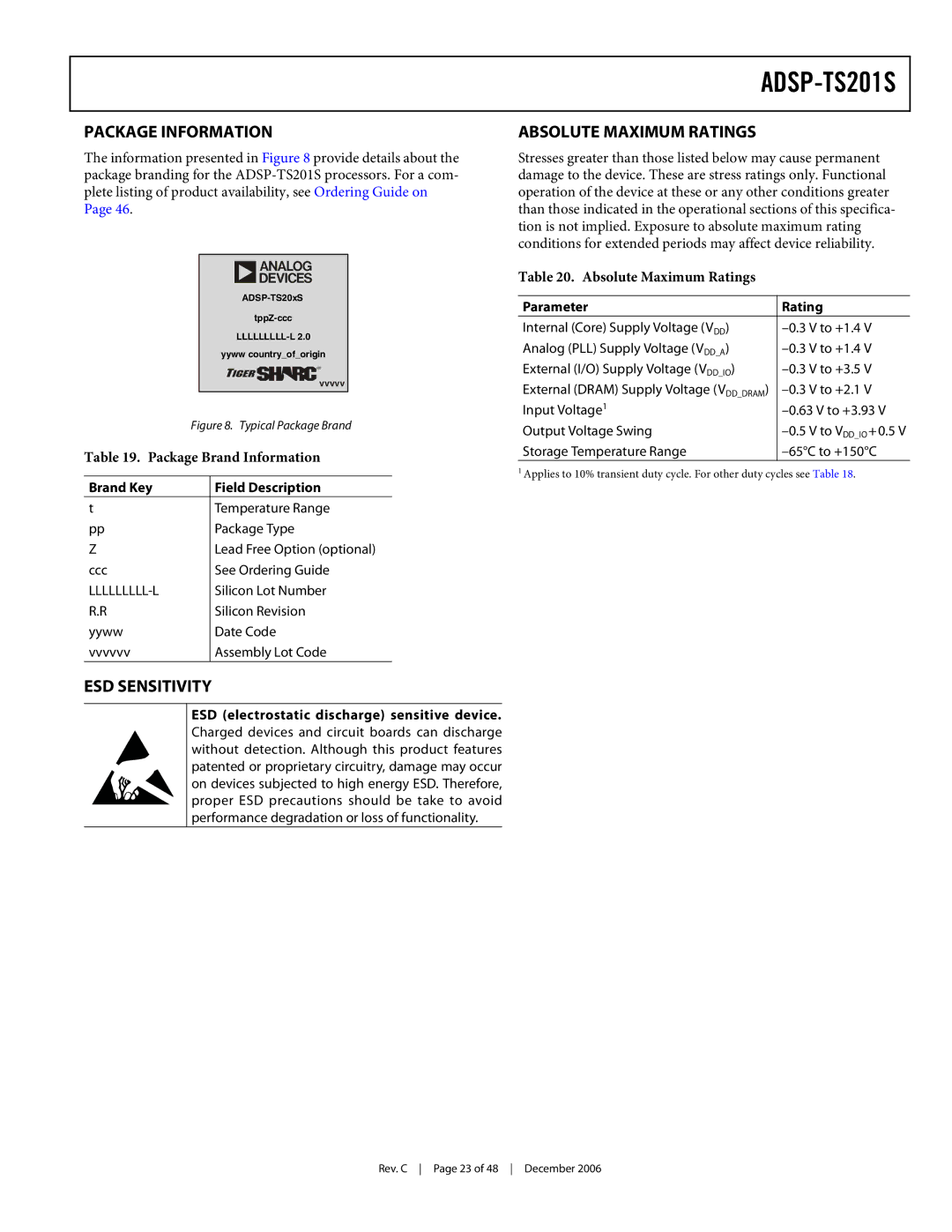
The information presented in Figure 8 provide details about the package branding for the
a
yyww country_of_origin
Tvvvvv
Figure 8. Typical Package Brand
Table 19. Package Brand Information
Brand Key | Field Description |
t | Temperature Range |
pp | Package Type |
Z | Lead Free Option (optional) |
ccc | See Ordering Guide |
Silicon Lot Number | |
R.R | Silicon Revision |
yyww | Date Code |
vvvvvv | Assembly Lot Code |
ESD SENSITIVITY
ESD (electrostatic discharge) sensitive device.
Charged devices and circuit boards can discharge without detection. Although this product features patented or proprietary circuitry, damage may occur on devices subjected to high energy ESD. Therefore, proper ESD precautions should be take to avoid performance degradation or loss of functionality.
ABSOLUTE MAXIMUM RATINGS
Stresses greater than those listed below may cause permanent damage to the device. These are stress ratings only. Functional operation of the device at these or any other conditions greater than those indicated in the operational sections of this specifica- tion is not implied. Exposure to absolute maximum rating conditions for extended periods may affect device reliability.
Table 20. Absolute Maximum Ratings
Parameter | Rating |
Internal (Core) Supply Voltage (VDD) | |
Analog (PLL) Supply Voltage (VDD_A) | |
External (I/O) Supply Voltage (VDD_IO) | |
External (DRAM) Supply Voltage (VDD_DRAM) | |
Input Voltage1 | |
Output Voltage Swing | |
Storage Temperature Range |
|
1Applies to 10% transient duty cycle. For other duty cycles see Table 18.
Rev. C Page 23 of 48 December 2006