ADSP-TS201S
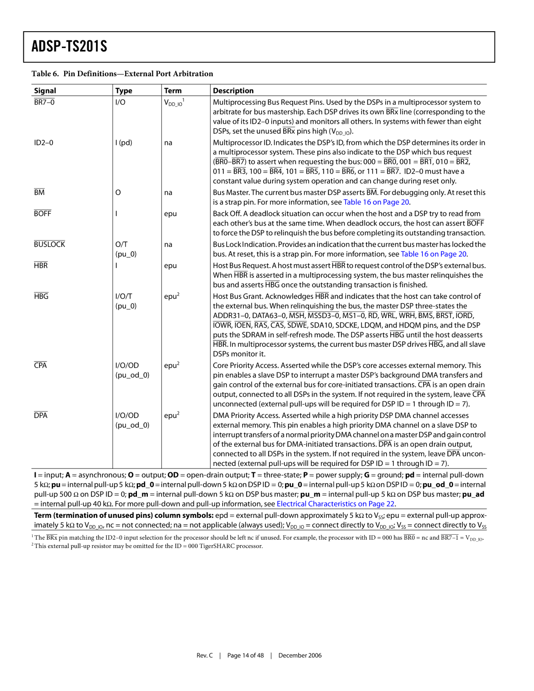
Table 6. Pin Definitions—External Port Arbitration
| Signal |
| Type | Term |
|
| Description | ||||||||||||||||||||||||||||||||||||||||||||||||||||||||||||||||||||||||||||||||
|
|
|
|
|
|
|
|
|
|
|
| 1 |
|
|
|
|
|
|
|
|
|
|
|
|
|
|
|
|
|
|
|
|
|
|
|
|
|
|
|
|
|
|
|
|
|
|
|
|
|
|
|
|
|
|
|
|
|
|
|
|
|
|
|
|
|
|
|
|
|
|
|
|
|
|
|
|
|
|
|
|
|
|
|
|
|
|
|
|
|
| I/O | VDD_IO |
| Multiprocessing Bus Request Pins. Used by the DSPs in a multiprocessor system to | |||||||||||||||||||||||||||||||||||||||||||||||||||||||||||||||||||||||||||||||||
|
|
|
| ||||||||||||||||||||||||||||||||||||||||||||||||||||||||||||||||||||||||||||||||||||
|
|
|
|
|
|
|
|
|
|
|
|
|
| arbitrate for bus mastership. Each DSP drives its own | BRx |
|
| line (corresponding to the | |||||||||||||||||||||||||||||||||||||||||||||||||||||||||||||||||||||
|
|
|
|
|
|
|
|
|
|
|
|
|
| value of its | |||||||||||||||||||||||||||||||||||||||||||||||||||||||||||||||||||||||||
|
|
|
|
|
|
|
|
|
|
|
|
|
| DSPs, set the unused |
|
|
|
| pins high (VDD_IO). | ||||||||||||||||||||||||||||||||||||||||||||||||||||||||||||||||||||
|
|
|
|
|
|
|
|
|
|
|
|
| BRx | ||||||||||||||||||||||||||||||||||||||||||||||||||||||||||||||||||||||||||
|
|
| I (pd) | na |
| Multiprocessor ID. Indicates the DSP’s ID, from which the DSP determines its order in | |||||||||||||||||||||||||||||||||||||||||||||||||||||||||||||||||||||||||||||||||
|
|
|
|
|
|
|
|
|
|
|
|
|
| a multiprocessor system. These pins also indicate to the DSP which bus request | |||||||||||||||||||||||||||||||||||||||||||||||||||||||||||||||||||||||||
|
|
|
|
|
|
|
|
|
|
|
|
|
|
|
|
|
|
|
|
|
|
|
|
|
|
|
|
|
|
|
|
|
|
|
|
|
|
|
|
|
|
|
|
|
|
|
|
|
|
|
|
|
|
|
|
|
|
|
|
|
|
|
|
|
|
|
|
|
|
|
|
|
|
|
|
|
|
|
|
|
|
|
| ||||
|
|
|
|
|
|
|
|
|
|
|
|
| |||||||||||||||||||||||||||||||||||||||||||||||||||||||||||||||||||||||||||
|
|
|
|
|
|
|
|
|
|
|
|
| 011 = | BR3, | 100 = | BR4, | 101 = |
| BR5, | 110 = | BR6, | or 111 = | BR7. | ||||||||||||||||||||||||||||||||||||||||||||||||||||||||||||||||
|
|
|
|
|
|
|
|
|
|
|
|
|
| constant value during system operation and can change during reset only. | |||||||||||||||||||||||||||||||||||||||||||||||||||||||||||||||||||||||||
|
|
|
|
|
|
|
|
| O | na |
| Bus Master. The current bus master DSP asserts |
|
|
|
| For debugging only. At reset this | ||||||||||||||||||||||||||||||||||||||||||||||||||||||||||||||||||||||
| BM |
| BM. | ||||||||||||||||||||||||||||||||||||||||||||||||||||||||||||||||||||||||||||||||||||
|
|
|
|
|
|
|
|
|
|
|
|
|
| is a strap pin. For more information, see Table 16 on Page 20. | |||||||||||||||||||||||||||||||||||||||||||||||||||||||||||||||||||||||||
|
|
|
|
|
|
|
| I | epu |
|
| Back Off. A deadlock situation can occur when the host and a DSP try to read from | |||||||||||||||||||||||||||||||||||||||||||||||||||||||||||||||||||||||||||
BOFF |
| ||||||||||||||||||||||||||||||||||||||||||||||||||||||||||||||||||||||||||||||||||||||
|
|
|
|
|
|
|
|
|
|
|
|
|
| each other’s bus at the same time. When deadlock occurs, the host can assert | BOFF |
|
| ||||||||||||||||||||||||||||||||||||||||||||||||||||||||||||||||||||||
|
|
|
|
|
|
|
|
|
|
|
|
|
| to force the DSP to relinquish the bus before completing its outstanding transaction. | |||||||||||||||||||||||||||||||||||||||||||||||||||||||||||||||||||||||||
|
|
|
|
|
|
| O/T | na |
|
| Bus Lock Indication. Provides an indication that the current bus master has locked the | ||||||||||||||||||||||||||||||||||||||||||||||||||||||||||||||||||||||||||||
| BUSLOCK |
| |||||||||||||||||||||||||||||||||||||||||||||||||||||||||||||||||||||||||||||||||||||
|
|
|
|
|
|
|
|
|
| (pu_0) |
|
|
| bus. At reset, this is a strap pin. For more information, see Table 16 on Page 20. | |||||||||||||||||||||||||||||||||||||||||||||||||||||||||||||||||||||||||
|
|
|
|
|
|
| I | epu |
|
| Host Bus Request. A host must assert |
|
|
| to request control of the DSP’s external bus. | ||||||||||||||||||||||||||||||||||||||||||||||||||||||||||||||||||||||||
HBR |
| HBR | |||||||||||||||||||||||||||||||||||||||||||||||||||||||||||||||||||||||||||||||||||||
|
|
|
|
|
|
|
|
|
|
|
|
|
| When | HBR | is asserted in a multiprocessing system, the bus master relinquishes the | |||||||||||||||||||||||||||||||||||||||||||||||||||||||||||||||||||||||
|
|
|
|
|
|
|
|
|
|
|
|
|
| bus and asserts | HBG | once the outstanding transaction is finished. | |||||||||||||||||||||||||||||||||||||||||||||||||||||||||||||||||||||||
|
|
|
|
|
| I/O/T | epu2 |
|
| Host Bus Grant. Acknowledges |
| and indicates that the host can take control of | |||||||||||||||||||||||||||||||||||||||||||||||||||||||||||||||||||||||||||
| HBG |
| HBR | ||||||||||||||||||||||||||||||||||||||||||||||||||||||||||||||||||||||||||||||||||||
|
|
|
|
|
|
|
|
|
| (pu_0) |
|
|
| the external bus. When relinquishing the bus, the master DSP | |||||||||||||||||||||||||||||||||||||||||||||||||||||||||||||||||||||||||
|
|
|
|
|
|
|
|
|
|
|
|
|
|
|
|
|
|
|
|
|
|
|
|
|
|
|
|
|
|
|
|
|
|
|
|
|
|
|
|
|
|
|
|
| |||||||||||||||||||||||||||||||||||||||||||
|
|
|
|
|
|
|
|
|
|
|
|
| MSH, | RD, | WRL, | WRH, | BMS, | BRST, | IORD, | ||||||||||||||||||||||||||||||||||||||||||||||||||||||||||||||||||||
|
|
|
|
|
|
|
|
|
|
|
|
|
| IOWR, |
| IOEN, |
| RAS, |
| CAS, |
| SDWE, | SDA10, SDCKE, LDQM, and HDQM pins, and the DSP | ||||||||||||||||||||||||||||||||||||||||||||||||||||||||||||||||
|
|
|
|
|
|
|
|
|
|
|
|
|
| puts the SDRAM in | HBG | until the host deasserts | |||||||||||||||||||||||||||||||||||||||||||||||||||||||||||||||||||||||
|
|
|
|
|
|
|
|
|
|
|
|
|
| HBR. | In multiprocessor systems, the current bus master DSP drives | HBG, | and all slave | ||||||||||||||||||||||||||||||||||||||||||||||||||||||||||||||||||||||
|
|
|
|
|
|
|
|
|
|
|
|
|
| DSPs monitor it. | |||||||||||||||||||||||||||||||||||||||||||||||||||||||||||||||||||||||||
|
|
|
|
| I/O/OD | epu2 |
|
| Core Priority Access. Asserted while the DSP’s core accesses external memory. This | ||||||||||||||||||||||||||||||||||||||||||||||||||||||||||||||||||||||||||||||
| CPA |
|
| ||||||||||||||||||||||||||||||||||||||||||||||||||||||||||||||||||||||||||||||||||||
|
|
|
|
|
|
|
|
|
| (pu_od_0) |
|
|
| pin enables a slave DSP to interrupt a master DSP’s background DMA transfers and | |||||||||||||||||||||||||||||||||||||||||||||||||||||||||||||||||||||||||
|
|
|
|
|
|
|
|
|
|
|
|
|
| gain control of the external bus for |
| is an open drain | |||||||||||||||||||||||||||||||||||||||||||||||||||||||||||||||||||||||
|
|
|
|
|
|
|
|
|
|
|
|
|
| CPA | |||||||||||||||||||||||||||||||||||||||||||||||||||||||||||||||||||||||||
|
|
|
|
|
|
|
|
|
|
|
|
|
| output, connected to all DSPs in the system. If not required in the system, leave | CPA |
| |||||||||||||||||||||||||||||||||||||||||||||||||||||||||||||||||||||||
|
|
|
|
|
|
|
|
|
|
|
|
|
| unconnected (external | |||||||||||||||||||||||||||||||||||||||||||||||||||||||||||||||||||||||||
|
|
|
| I/O/OD | epu2 |
|
| DMA Priority Access. Asserted while a high priority DSP DMA channel accesses | |||||||||||||||||||||||||||||||||||||||||||||||||||||||||||||||||||||||||||||||
| DPA |
|
| ||||||||||||||||||||||||||||||||||||||||||||||||||||||||||||||||||||||||||||||||||||
|
|
|
|
|
|
|
|
|
| (pu_od_0) |
|
|
| external memory. This pin enables a high priority DMA channel on a slave DSP to | |||||||||||||||||||||||||||||||||||||||||||||||||||||||||||||||||||||||||
|
|
|
|
|
|
|
|
|
|
|
|
|
| interrupt transfers of a normal priority DMA channel on a master DSP and gain control | |||||||||||||||||||||||||||||||||||||||||||||||||||||||||||||||||||||||||
|
|
|
|
|
|
|
|
|
|
|
|
|
| of the external bus for |
| is an open drain output, | |||||||||||||||||||||||||||||||||||||||||||||||||||||||||||||||||||||||
|
|
|
|
|
|
|
|
|
|
|
|
|
| DPA | |||||||||||||||||||||||||||||||||||||||||||||||||||||||||||||||||||||||||
|
|
|
|
|
|
|
|
|
|
|
|
|
| connected to all DSPs in the system. If not required in the system, leave | DPA | uncon- | |||||||||||||||||||||||||||||||||||||||||||||||||||||||||||||||||||||||
|
|
|
|
|
|
|
|
|
|
|
|
|
| nected (external | |||||||||||||||||||||||||||||||||||||||||||||||||||||||||||||||||||||||||
I = input; A = asynchronous; O = output; OD =
5kΩ; pu = internal
Term (termination of unused pins) column symbols: epd = external
1The BRx pin matching the
2 This external
Rev. C Page 14 of 48 December 2006