ADSP-TS201S
Table 29. AC Signal Specifications (Continued)
(All values in this table are in nanoseconds.)
Name | Description | SetupInput (Min) | HoldInput (Min) | OutputValid (Max) | OutputHold (Min) | OutputEnable (Min) | OutputDisable (Max) | Reference Clock |
|
|
|
|
|
| 1 | 1 |
|
|
|
|
|
|
|
|
|
|
| Static | — | — | — | — | — | — | — |
| Static | — | — | — | — | — | — | — |
ENEDREG | Static | — | — | — | — | — | — | — |
STRAP SYS9, 10 | Strap Pins | 1.5 | 0.5 | — | — | — | — | SCLK |
JTAG SYS11, 12 | JTAG System Pins | +2.5 | +10.0 | +12.0 | — | — | TCK |
1The external port protocols employ bus IDLE cycles for bus mastership transitions as well as slave access boundary crossings to avoid any potential bus contention. The apparent driver overlap, due to output disables being larger than output enables, is not actual.
2For input specifications on
3These input pins are asynchronous and therefore do not need to be synchronized to a clock reference.
4 For additional requirement details, see Reset and Booting on Page 9.
5 RST_IN clock reference is the falling edge of SCLK.
6 TDO output clock reference is the falling edge of TCK.
7 Reference clock depends on function.
8 These pins may change only during reset; recommend connecting it to VDD_IO/VSS.
9 STRAP pins include: BMS, BM, BUSLOCK, TMR0E, L1BCMPO, L2BCMPO, and L3BCMPO.
10Specifications applicable during reset only.
11JTAG system pins include: RST_IN, RST_OUT, POR_IN,
12JTAG system output timing clock reference is the falling edge of TCK.
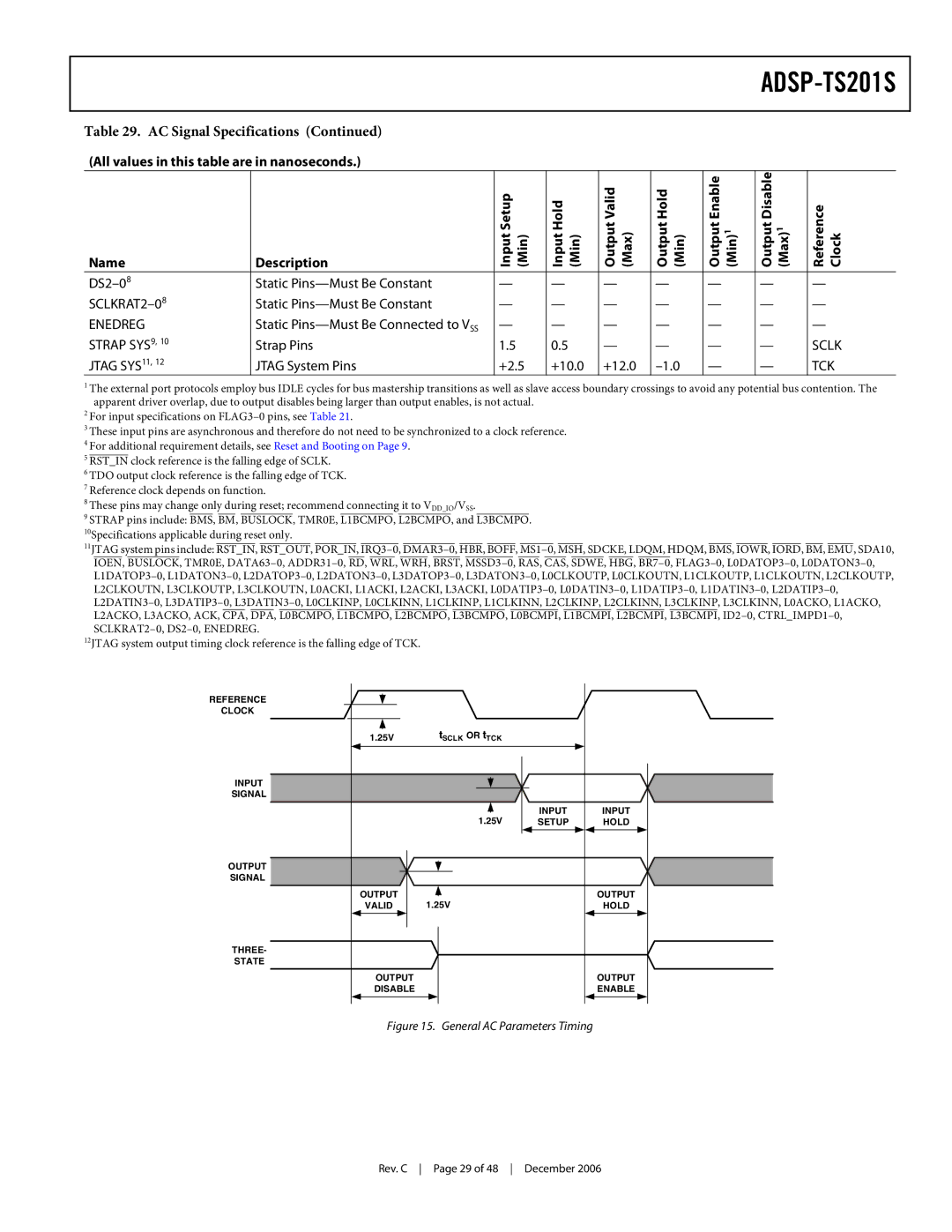
REFERENCE |
|
|
CLOCK |
|
|
1.25V | tSCLK OR tTCK |
|
INPUT |
|
|
SIGNAL |
|
|
| 1.25V | INPUT |
| SETUP | |
OUTPUT |
|
|
SIGNAL |
|
|
OUTPUT | 1.25V |
|
VALID |
| |
THREE- |
|
|
STATE |
|
|
OUTPUT |
|
|
DISABLE |
|
|
INPUT
HOLD
OUTPUT
HOLD
OUTPUT ENABLE
Figure 15. General AC Parameters Timing
Rev. C Page 29 of 48 December 2006