ADSP-TS201S
INTERNAL SPACE
RESERVED
SOC REGISTERS (UREGS)
RESERVED
INTERNAL REGISTERS (UREGS)
RESERVED
INTERNAL MEMORY BLOCK 10
RESERVED
INTERNAL MEMORY BLOCK 8
RESERVED
INTERNAL MEMORY BLOCK 6
RESERVED
INTERNAL MEMORY BLOCK 4
RESERVED
INTERNAL MEMORY BLOCK 2
RESERVED
INTERNAL MEMORY BLOCK 0
0x03FFFFFF
0x001F03FF
0x001F0000
0x001E03FF
0x001E0000
0x0015FFFF
0x00140000
0x0011FFFF
0x00100000
0x000DFFFF
0x000C0000
0x0009FFFF
0x00080000
0x0005FFFF
0x00040000
0x0001FFFF
0x00000000
| GLOBAL SPACE | |
| HOST (MSH) | |
|
| |
| RESERVED | |
| MSSD BANK 3 (MSSD3) | |
|
| |
| RESERVED | |
SPACE | MSSD BANK 2 (MSS D2) | |
| ||
|
| |
MEMORY | RESERVED | |
MSSD BANK 1 (MSSD1) | ||
| ||
|
| |
EXTERNAL | RESERVED | |
MSSD BANK 0 (MSSD0) | ||
| ||
|
| |
| BANK 1 (MS 1) | |
|
| |
| BANK 0 (MS 0) | |
|
| |
SPACE | PROCESSOR ID 7 | |
| ||
PROCESSOR ID 6 | ||
MEMORY |
| |
PROCESSOR ID 5 | ||
|
| |
| PROCESSOR ID 4 | |
MULTIPROCESSOR |
| |
PROCESSOR ID 3 | ||
|
| |
| PROCESSOR ID 2 | |
|
| |
| PROCESSOR ID 1 | |
|
| |
| PROCESSOR ID 0 | |
|
| |
| BROADCAST | |
|
| |
| RESERVED | |
|
| |
| INTERNAL MEMORY | |
|
|
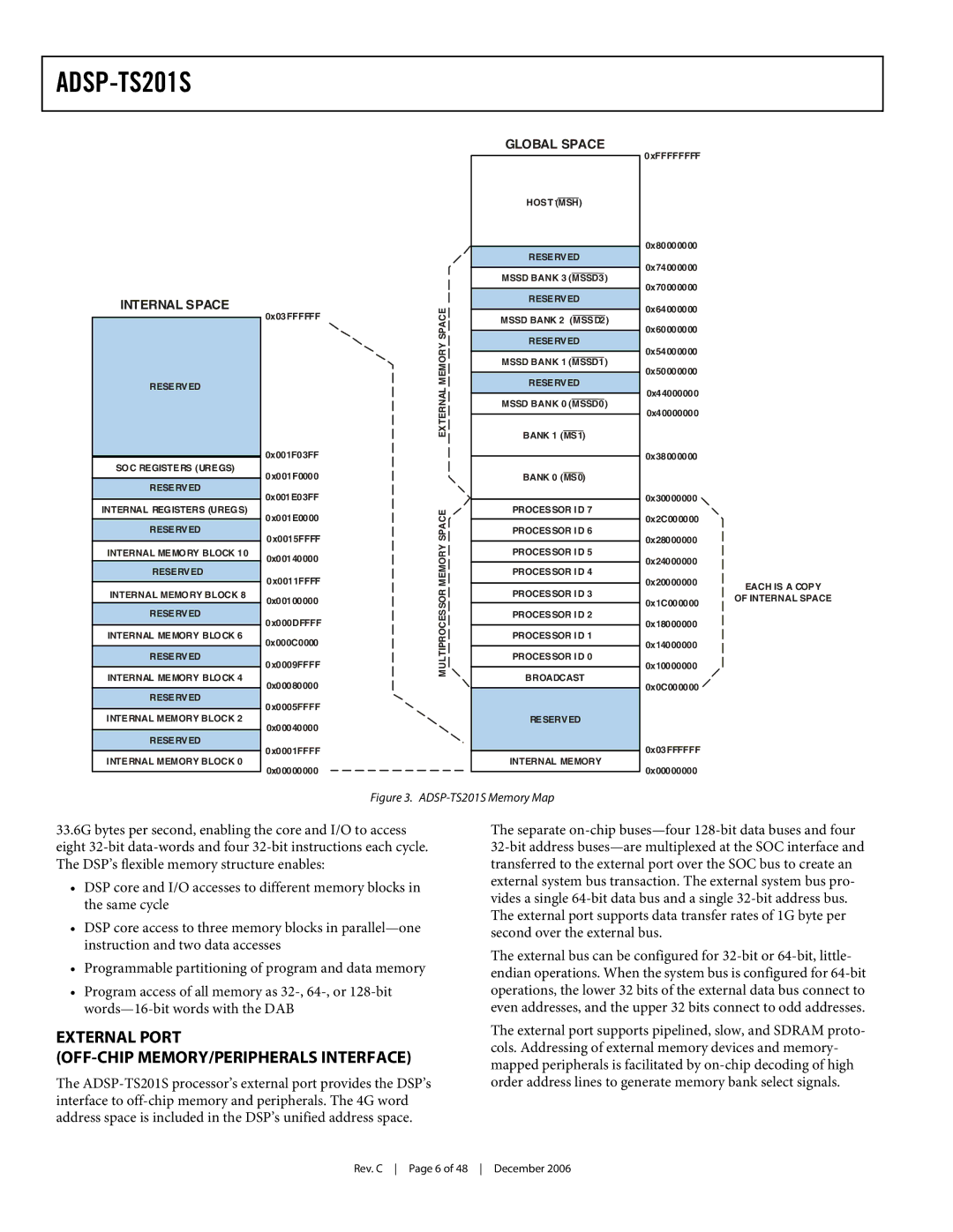
Figure 3. ADSP-TS201S Memory Map
0xFFFFFFFF
0x80000000
0x74000000
0x70000000
0x64000000
0x60000000
0x54000000
0x50000000
0x44000000
0x40000000
0x38000000
0x30000000
0x2C000000
0x28000000
0x24000000
0x20000000
0x1C000000
0x18000000
0x14000000
0x10000000
0x0C000000
0x03FFFFFF
0x00000000
EACH IS A COPY
OF INTERNAL SPACE
33.6G bytes per second, enabling the core and I/O to access eight
•DSP core and I/O accesses to different memory blocks in the same cycle
•DSP core access to three memory blocks in
•Programmable partitioning of program and data memory
•Program access of all memory as
EXTERNAL PORT
(OFF-CHIP MEMORY/PERIPHERALS INTERFACE)
The
The separate
The external bus can be configured for
The external port supports pipelined, slow, and SDRAM proto- cols. Addressing of external memory devices and memory- mapped peripherals is facilitated by
Rev. C Page 6 of 48 December 2006