ADSP-TS201S
TIMING SPECIFICATIONS
With the exception of
General AC Timing
Timing is measured on signals when they cross the 1.25 V level as described in Figure 15 on Page 29. All delays (in nanosec- onds) are measured between the point that the first signal reaches 1.25 V and the point that the second signal reaches 1.25 V.
Table 21. AC Asynchronous Signal Specifications
The general ac timing data appears in Table 22 and Table 29. All ac specifications are measured with the load specified in Figure 36 on Page 38, and with the output drive strength set to strength 4. In order to calculate the output valid and hold times for different load conditions and/or output drive strengths, refer to Figure 37 on Page 38 through Figure 44 on Page 39 (Rise and Fall Time vs. Load Capacitance) and Figure 45 on Page 39 (Out- put Valid vs. Load Capacitance and Drive Strength).
The ac asynchronous timing data for the
| Name | Description | Pulse Width Low (Min) | Pulse Width High (Min) | ||
|
| 1 |
| Interrupt Request | 2 × tSCLK ns | 2 × tSCLK ns |
| ||||||
|
| 1 | DMA Request | 2 × tSCLK ns | 2 × tSCLK ns | |
| ||||||
| 2×tSCLK ns | 2×tSCLK ns | ||||
| TMR0E3 | Timer 0 Expired | 4×tSCLK ns | — | ||
1These input pins have Schmitt triggers and therefore do not need to be synchronized to a clock reference.
2 For output specifications on
3 This pin is a strap option. During reset, an internal resistor pulls the pin low.
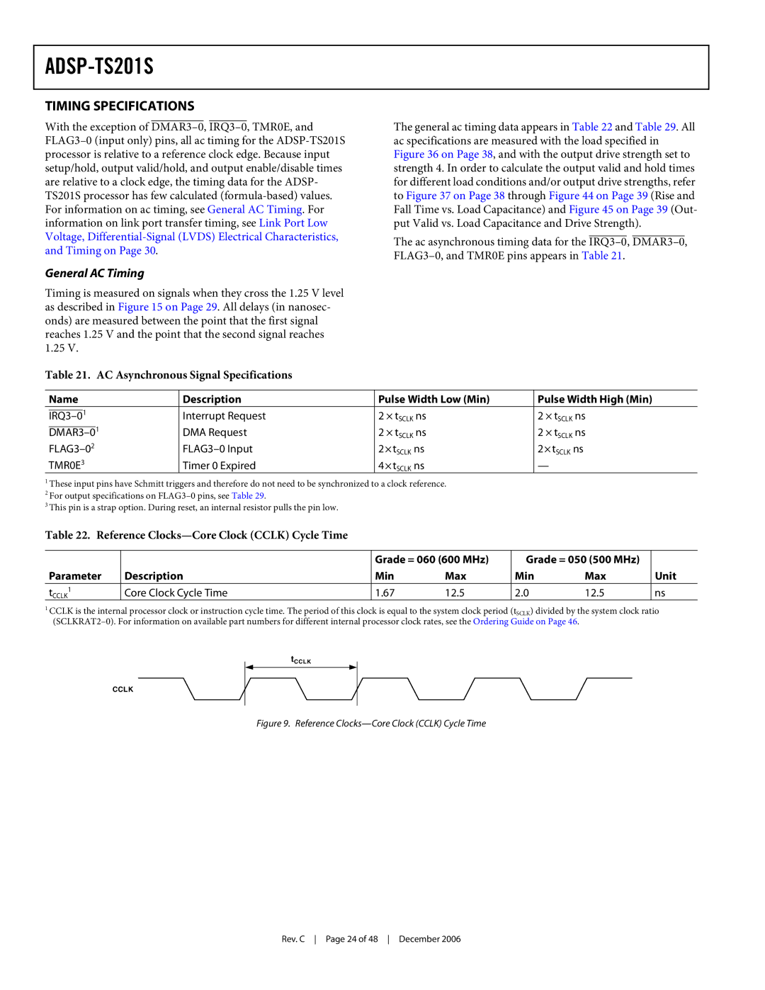
Table 22. Reference Clocks—Core Clock (CCLK) Cycle Time
|
| Grade = 060 (600 MHz) | Grade = 050 (500 MHz) |
| ||
Parameter | Description | Min | Max | Min | Max | Unit |
1 | Core Clock Cycle Time | 1.67 | 12.5 | 2.0 | 12.5 | ns |
tCCLK | ||||||
1CCLK is the internal processor clock or instruction cycle time. The period of this clock is equal to the system clock period (tSCLK) divided by the system clock ratio
tCCLK
CCLK
Figure 9. Reference Clocks—Core Clock (CCLK) Cycle Time
Rev. C Page 24 of 48 December 2006