ADSP-TS201S
ADSP-TS201S—SPECIFICATIONS
Note that component specifications are subject to change with- out notice. For information on link port electrical characteristics, see Link Port Low Voltage,
OPERATING CONDITIONS
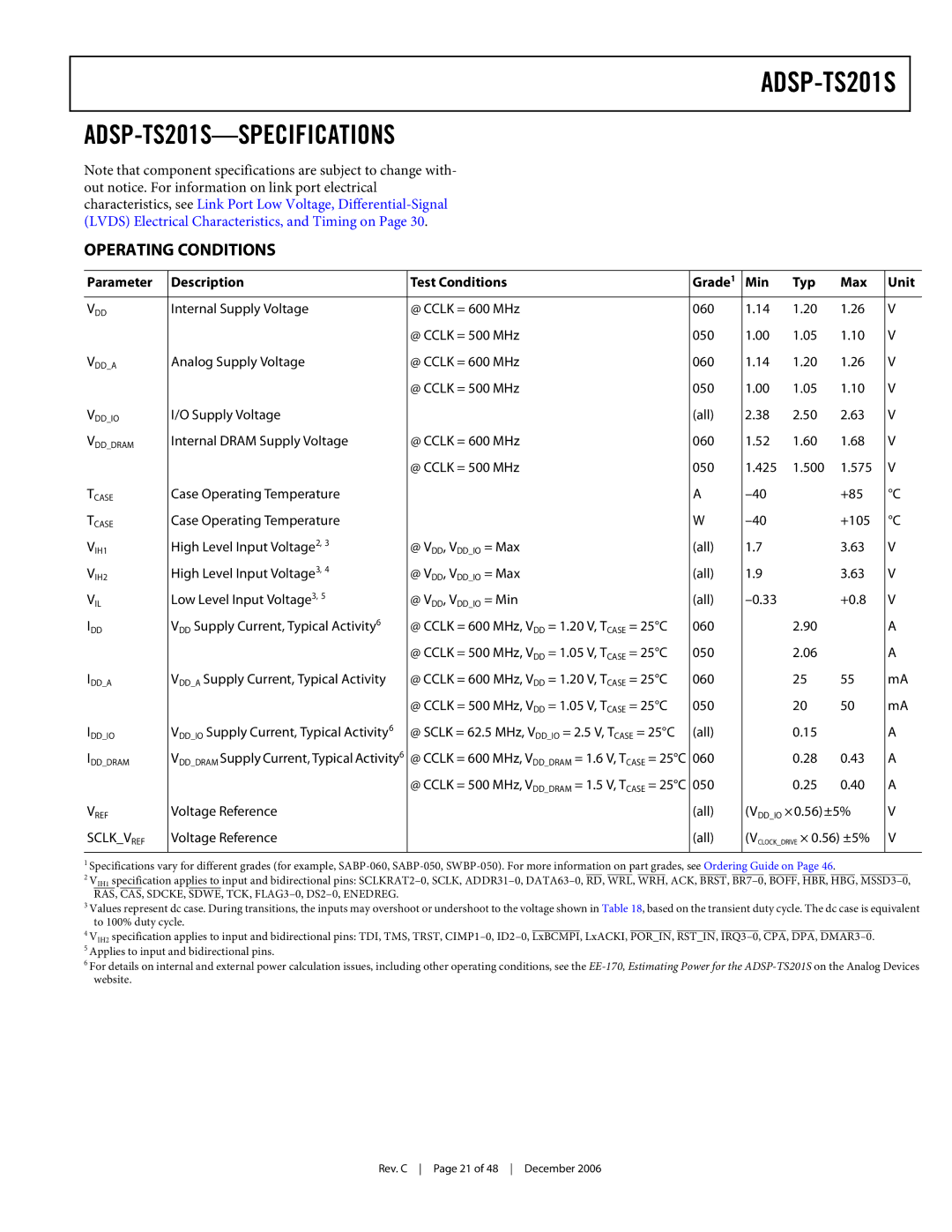
Parameter | Description | Test Conditions | Grade1 | Min | Typ | Max | Unit |
|
|
|
|
|
|
|
|
VDD | Internal Supply Voltage | @ CCLK = 600 MHz | 060 | 1.14 | 1.20 | 1.26 | V |
|
| @ CCLK = 500 MHz | 050 | 1.00 | 1.05 | 1.10 | V |
VDD_A | Analog Supply Voltage | @ CCLK = 600 MHz | 060 | 1.14 | 1.20 | 1.26 | V |
|
| @ CCLK = 500 MHz | 050 | 1.00 | 1.05 | 1.10 | V |
VDD_IO | I/O Supply Voltage |
| (all) | 2.38 | 2.50 | 2.63 | V |
VDD_DRAM | Internal DRAM Supply Voltage | @ CCLK = 600 MHz | 060 | 1.52 | 1.60 | 1.68 | V |
|
| @ CCLK = 500 MHz | 050 | 1.425 | 1.500 | 1.575 | V |
TCASE | Case Operating Temperature |
| A |
| +85 | °C | |
TCASE | Case Operating Temperature |
| W |
| +105 | °C | |
VIH1 | High Level Input Voltage2, 3 | @ VDD, VDD_IO = Max | (all) | 1.7 |
| 3.63 | V |
VIH2 | High Level Input Voltage3, 4 | @ VDD, VDD_IO = Max | (all) | 1.9 |
| 3.63 | V |
VIL | Low Level Input Voltage3, 5 | @ VDD, VDD_IO = Min | (all) |
| +0.8 | V | |
IDD | VDD Supply Current, Typical Activity6 | @ CCLK = 600 MHz, VDD = 1.20 V, TCASE = 25°C | 060 |
| 2.90 |
| A |
|
| @ CCLK = 500 MHz, VDD = 1.05 V, TCASE = 25°C | 050 |
| 2.06 |
| A |
IDD_A | VDD_A Supply Current, Typical Activity | @ CCLK = 600 MHz, VDD = 1.20 V, TCASE = 25°C | 060 |
| 25 | 55 | mA |
|
| @ CCLK = 500 MHz, VDD = 1.05 V, TCASE = 25°C | 050 |
| 20 | 50 | mA |
IDD_IO | VDD_IO Supply Current, Typical Activity6 | @ SCLK = 62.5 MHz, VDD_IO = 2.5 V, TCASE = 25°C | (all) |
| 0.15 |
| A |
IDD_DRAM | VDD_DRAM Supply Current, Typical Activity6 | @ CCLK = 600 MHz, VDD_DRAM = 1.6 V, TCASE = 25°C | 060 |
| 0.28 | 0.43 | A |
|
| @ CCLK = 500 MHz, VDD_DRAM = 1.5 V, TCASE = 25°C | 050 |
| 0.25 | 0.40 | A |
VREF | Voltage Reference |
| (all) | (VDD_IO ×0.56)±5% | V | ||
SCLK_VREF | Voltage Reference |
| (all) | (VCLOCK_DRIVE × 0.56) ±5% | V | ||
|
|
|
|
|
|
|
|
1Specifications vary for different grades (for example,
2VIH1 specification applies to input and bidirectional pins:
3Values represent dc case. During transitions, the inputs may overshoot or undershoot to the voltage shown in Table 18, based on the transient duty cycle. The dc case is equivalent to 100% duty cycle.
4VIH2 specification applies to input and bidirectional pins: TDI, TMS, TRST,
5 Applies to input and bidirectional pins.
6 For details on internal and external power calculation issues, including other operating conditions, see the
Rev. C Page 21 of 48 December 2006