ADSP-TS201S
Output Enable Time
Output pins are considered to be enabled when they have made a transition from a high impedance state to when they start driv- ing. The time for the voltage on the bus to ramp by ΔV is dependent on the capacitive load, CL, and the drive current, ID. This ramp time can be approximated by the following equation:
tRAMP = (CLΔV) ⁄ ID
The output enable time tENA is the difference between
tMEASURED_ENA and tRAMP as shown in Figure 35. The time
tMEASURED_ENA is the interval from when the reference signal switches to when the output voltage ramps ΔV from the mea-
sured
Capacitive Loading
Output valid and hold are based on standard capacitive loads: 30 pF on all pins (see Figure 36). The delay and hold specifica- tions given should be derated by a drive strength related factor for loads other than the nominal value of 30 pF. Figure 37 through Figure 44 show how output rise time varies with capac- itance. Figure 45 graphically shows how output valid varies with load capacitance. (Note that this graph or derating does not apply to output disable delays; see Output Disable Time on Page 37.) The graphs of Figure 37 through Figure 45 may not be linear outside the ranges shown.
TO | 50Ω |
OUTPUT | 1.25V |
PIN | 30pF |
|
Figure 36. Equivalent Device Loading for AC Measurements (Includes All Fixtures)
|
|
|
|
| STRENGTH 0 |
|
|
|
| ||
| 25 |
|
|
| (VDD_IO = 2.5V) |
|
|
|
| ||
|
|
|
|
|
|
|
|
|
|
| |
(ns) | 20 |
|
|
|
|
|
|
|
|
|
|
TIMES |
|
|
|
|
|
|
|
|
|
| |
| FALL TIME |
|
|
|
|
|
|
| |||
FALL | 15 |
|
|
|
|
|
|
| |||
Y = 0.251x + 4.2245 |
|
|
|
|
|
| |||||
|
|
|
|
|
|
| |||||
AND | 10 |
|
|
|
|
|
|
|
|
|
|
RISE |
|
|
| RISE TIME |
|
|
|
| |||
|
|
|
|
|
|
|
| ||||
|
|
|
| Y = 0.259x + 3.0842 |
|
|
|
| |||
|
|
|
|
|
|
|
|
| |||
| 5 |
|
|
|
|
|
|
|
|
|
|
| 0 | 10 | 20 | 30 | 40 | 50 | 60 | 70 | 80 | 90 | 100 |
| 0 | ||||||||||
|
|
|
| LOAD CAPACITANCE (pF) |
|
|
| ||||
Figure 37. Typical Output Rise and Fall Time (10% to 90%, VDD_IO = 2.5 V) vs. Load Capacitance at Strength 0
|
|
|
|
|
| STRENGTH 1 |
|
|
|
| |
| 25 |
|
|
| (VDD_IO = 2.5V) |
|
|
|
| ||
|
|
|
|
|
|
|
|
|
|
| |
(ns) |
|
|
|
|
|
|
|
|
|
|
|
FALLTIMES | 20 |
|
|
|
|
|
|
|
|
|
|
15 |
|
| FALL TIME |
|
|
|
|
| |||
AND |
|
|
|
|
|
|
|
| |||
|
|
| Y = 0.1527x + 0.7485 |
|
|
|
| ||||
RISE |
|
|
|
|
|
|
| ||||
10 |
|
|
|
|
|
|
|
|
|
| |
|
|
|
|
|
|
|
|
|
|
| |
| 5 |
|
|
|
|
| RISE TIME |
|
| ||
|
|
|
|
|
| Y = 0.1501x + 0.05 |
|
| |||
|
|
|
|
|
|
|
|
| |||
| 0 | 10 | 20 | 30 | 40 | 50 | 60 | 70 | 80 | 90 | 100 |
| 0 | ||||||||||
|
|
|
| LOAD CAPACITANCE (pF) |
|
|
| ||||
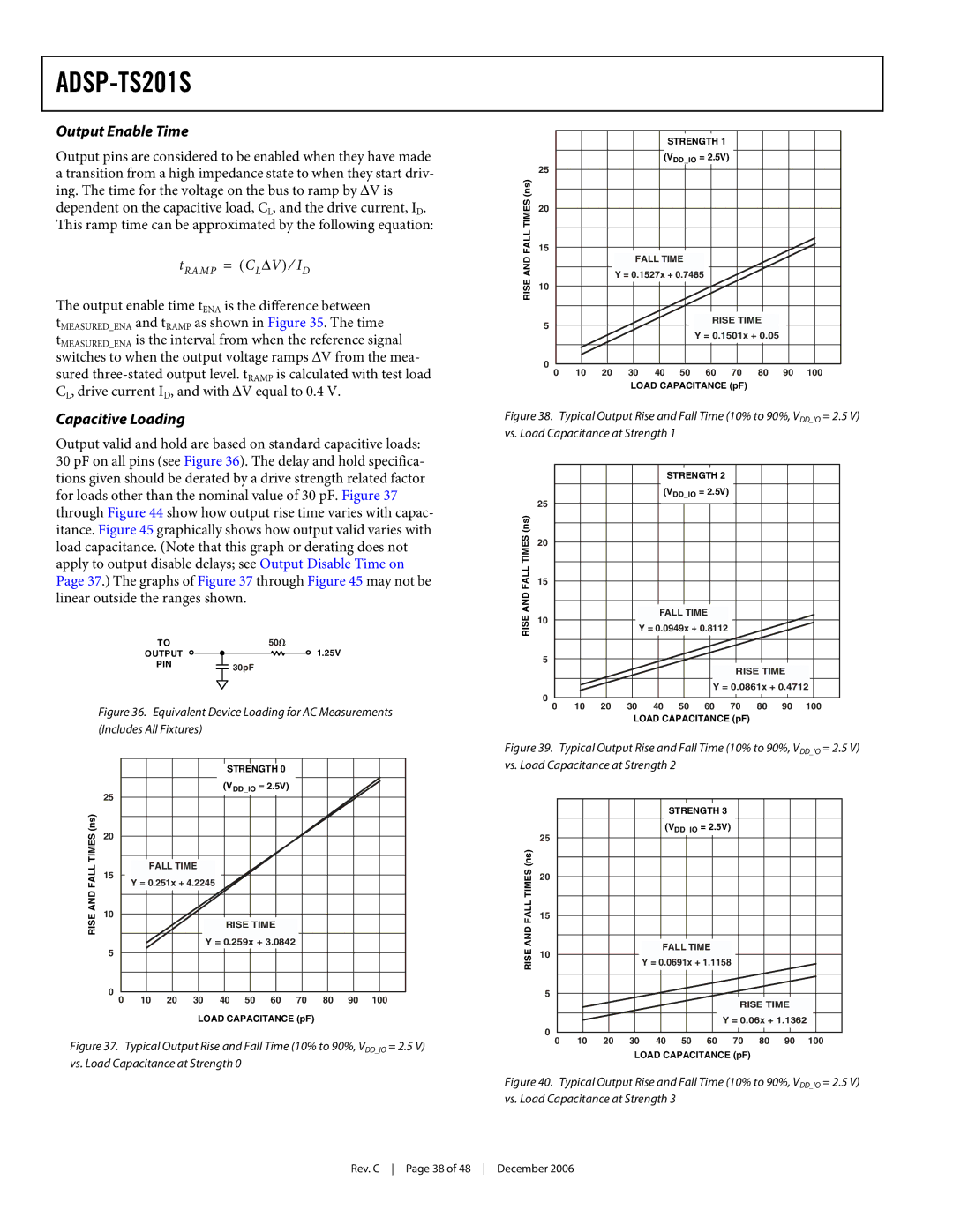
Figure 38. Typical Output Rise and Fall Time (10% to 90%, VDD_IO = 2.5 V) vs. Load Capacitance at Strength 1
|
|
|
|
|
| STRENGTH 2 |
|
|
|
| |
| 25 |
|
|
|
| (VDD_IO = 2.5V) |
|
|
|
| |
|
|
|
|
|
|
|
|
|
|
| |
(ns) |
|
|
|
|
|
|
|
|
|
|
|
TIMES | 20 |
|
|
|
|
|
|
|
|
|
|
|
|
|
|
|
|
|
|
|
|
| |
ANDFALL | 15 |
|
|
|
|
|
|
|
|
|
|
|
|
|
| FALL TIME |
|
|
|
| |||
RISE | 10 |
|
|
|
|
|
|
| |||
|
|
| Y = 0.0949x + 0.8112 |
|
|
|
| ||||
|
|
|
|
|
|
|
| ||||
|
|
|
|
|
|
|
|
|
|
| |
| 5 |
|
|
|
|
|
|
|
|
|
|
|
|
|
|
|
|
|
| RISE TIME |
| ||
|
|
|
|
|
|
| Y = 0.0861x + 0.4712 | ||||
| 0 | 10 | 20 | 30 | 40 | 50 | 60 | 70 | 80 | 90 | 100 |
| 0 | ||||||||||
|
|
|
| LOAD CAPACITANCE (pF) |
|
|
| ||||
Figure 39. Typical Output Rise and Fall Time (10% to 90%, VDD_IO = 2.5 V) vs. Load Capacitance at Strength 2
STRENGTH 3
(VDD_IO = 2.5V)
| 25 |
|
|
|
|
|
|
|
|
|
|
(ns) |
|
|
|
|
|
|
|
|
|
|
|
TIMES | 20 |
|
|
|
|
|
|
|
|
|
|
|
|
|
|
|
|
|
|
|
|
| |
ANDFALL | 15 |
|
|
|
|
|
|
|
|
|
|
|
|
|
| FALL TIME |
|
|
|
| |||
RISE | 10 |
|
|
|
|
|
|
| |||
|
|
| Y = 0.0691x + 1.1158 |
|
|
| |||||
|
|
|
|
|
|
| |||||
|
|
|
|
|
|
|
|
|
|
| |
| 5 |
|
|
|
|
|
|
|
|
|
|
|
|
|
|
|
|
|
| RISE TIME |
| ||
|
|
|
|
|
|
|
| Y = 0.06x + 1.1362 |
| ||
| 0 | 10 | 20 | 30 | 40 | 50 | 60 | 70 | 80 | 90 | 100 |
| 0 | ||||||||||
|
|
|
| LOAD CAPACITANCE (pF) |
|
|
| ||||