ADSP-TS201S
LINK PORTS (LVDS)
The DSP’s four
per second.
The link ports provide an optional communications channel that is useful in multiprocessor systems for implementing point-
Each link port has its own
Each link port direction has three signals that control its opera- tion. For the transmitter, LxCLKOUT is the output transmit clock, LxACKI is the handshake input to control the data flow, and the LxBCMPO output indicates that the block transfer is complete. For the receiver, LxCLKIN is the input receive clock, LxACKO is the handshake output to control the data flow, and the LxBCMPI input indicates that the block transfer is com- plete. The
Applications can program separate error detection mechanisms for transmit and receive operations (applications can use the checksum mechanism to implement consecutive link port transfers), the size of data packets, and the speed at which bytes are transmitted.
TIMER AND GENERAL-PURPOSE I/O
The
RESET AND BOOTING
The
•
•Normal reset – for any chip reset following the
•
For normal operations, tie the RST_OUT pin to the POR_IN pin.
After reset, the
•Boot from EPROM.
•Boot by an external master (host or another
•Boot by link port.
•No
Using the “no boot” option, the
Table 2. No Boot, Run from Memory Addresses
| Interrupt | Address |
| |
|
|
| 0x3000 0000 | (External Memory) |
| IRQ0 | |||
|
|
| 0x3800 0000 | (External Memory) |
| IRQ1 | |||
|
|
| 0x8000 0000 | (External Memory) |
| IRQ2 | |||
|
|
| 0x0000 0000 | (Internal Memory) |
| IRQ3 | |||
The
For more information on boot options, see the
CLOCK DOMAINS
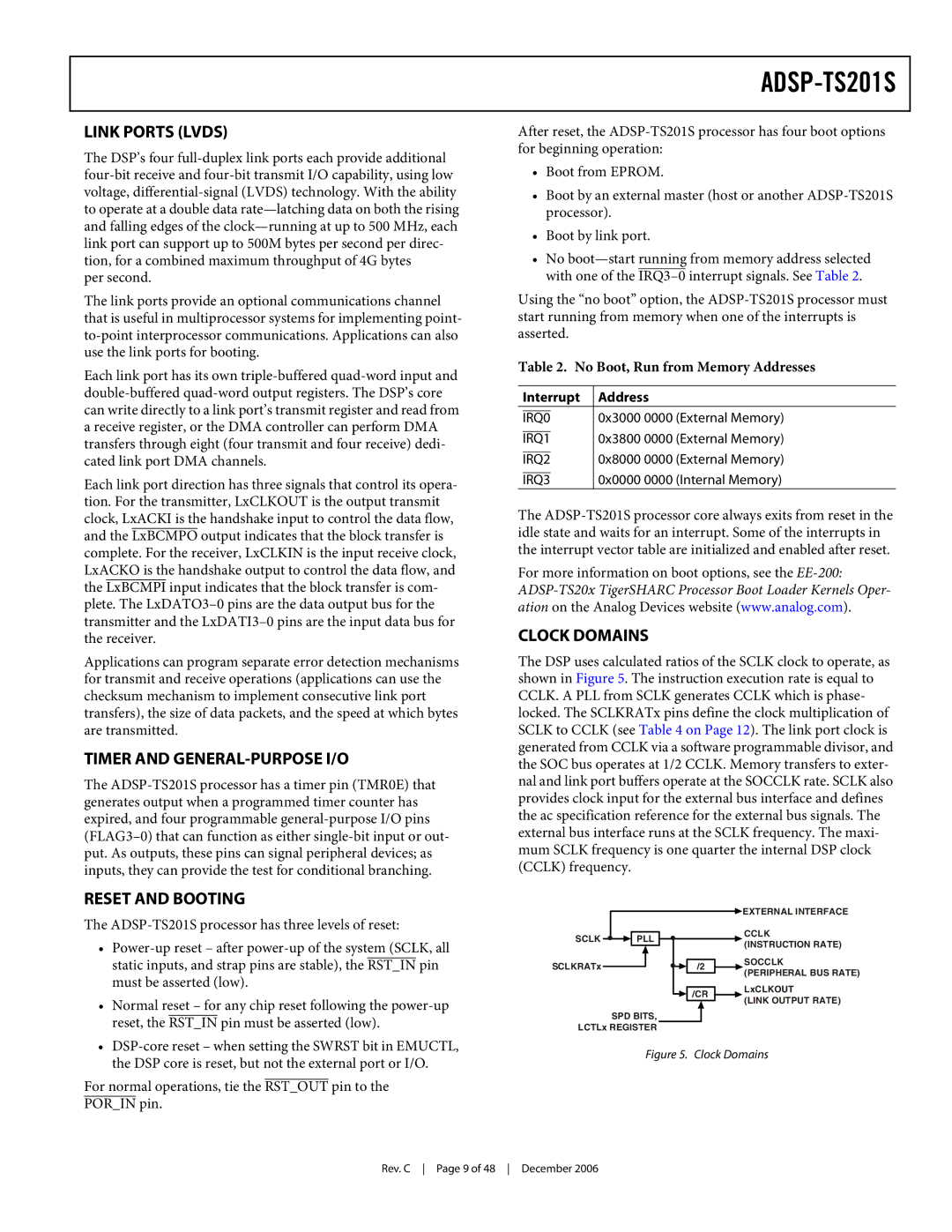
The DSP uses calculated ratios of the SCLK clock to operate, as shown in Figure 5. The instruction execution rate is equal to CCLK. A PLL from SCLK generates CCLK which is phase- locked. The SCLKRATx pins define the clock multiplication of SCLK to CCLK (see Table 4 on Page 12). The link port clock is generated from CCLK via a software programmable divisor, and the SOC bus operates at 1/2 CCLK. Memory transfers to exter- nal and link port buffers operate at the SOCCLK rate. SCLK also provides clock input for the external bus interface and defines the ac specification reference for the external bus signals. The external bus interface runs at the SCLK frequency. The maxi- mum SCLK frequency is one quarter the internal DSP clock (CCLK) frequency.
|
|
| EXTERNAL INTERFACE |
SCLK | PLL |
| CCLK |
| (INSTRUCTION RATE) | ||
|
|
| |
SCLKRATx |
| /2 | SOCCLK |
| (PERIPHERAL BUS RATE) | ||
|
|
| |
|
| /CR | LxCLKOUT |
|
| (LINK OUTPUT RATE) | |
|
|
| |
| SPD BITS, |
|
|
LCTLx REGISTER |
|
| |
Figure 5. Clock Domains
Rev. C Page 9 of 48 December 2006