ADSP-TS201S
FIRST EDGE OF 5TH SHORT WORD IN A QUAD WORD
LxCLKOUT
VOD = 0V
LxDATO
VOD = 0V
LxACKI
LxBCMPO
tLACKIS |
tBCMPOH |
LAST EDGE IN A QUAD WORD
tLACKIH
LxCLKOUT
VOD = 0V
LxDATO
VOD = 0V
LxACKI
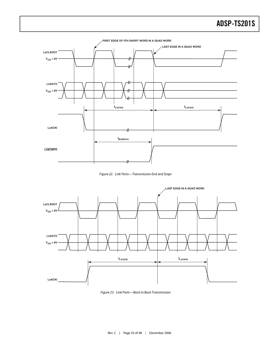
Figure 22. Link Ports—Transmission End and Stops
LAST EDGE IN A QUAD WORD
|
|
|
|
|
|
|
|
|
|
| tLACKIS |
|
| tLACKIH | |||
|
|
|
|
|
|
|
|
|
Figure 23. Link Ports—Back to Back Transmission
Rev. C Page 33 of 48 December 2006