Chapter 6
The RTC of the main controller is not found.
The battery capacity is low.
<Probable fault location> Lithium battery or main controller
<Countermeasure>
1)Start up the printer in the service mode, and then turn off the power.
2)Replace the lithium battery.
3)Replace the main controller
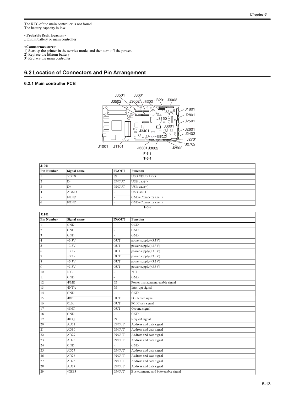
6.2 Location of Connectors and Pin Arrangement
6.2.1 Main controller PCB
|
| J3501 | J3601 |
| |
|
| J3502 | J3602 | J3202 J3201 J3003 | |
|
|
|
|
| J1801 |
|
|
|
|
| J2801 |
|
|
|
| J3150 | |
|
|
|
|
| J2501 |
|
|
|
|
| J3001 |
|
|
| J3401 | J2601 | |
|
|
| J2402 | ||
|
|
|
|
| |
|
|
|
|
| J2701 |
| J1001 | J1101 |
|
| J2702 |
| J3301 J3002 | J2502 | |||
|
|
| |||
|
|
|
|
| |
|
|
|
|
| |
J1001 |
|
|
|
|
|
Pin Number | Signal name | IN/OUT | Function |
| |
1 | VBUS | IN | USB VBUS(+5V) |
| |
2 | D- | IN/OUT | USB |
| |
3 | D+ | IN/OUT | USB data(+) |
| |
4 | AGND | - | USB GND |
| |
5 | FGND | - | GND (Connector shell) |
| |
6 | FGND | - | GND (Connector shell) |
| |
|
|
|
|
| |
J1101 |
|
|
|
|
|
Pin Number | Signal name | IN/OUT | Function |
| |
1 | GND | - | GND |
|
|
2 | GND | - | GND |
|
|
3 | GND | - | GND |
|
|
4 | +3.3V | OUT | power supply(+3.3V) |
| |
5 | +3.3V | OUT | power supply(+3.3V) |
| |
6 | +3.3V | OUT | power supply(+3.3V) |
| |
7 | +3.3V | OUT | power supply(+3.3V) |
| |
8 | +3.3V | OUT | power supply(+3.3V) |
| |
9 | +3.3V | OUT | power supply(+3.3V) |
| |
10 | N.C. | - | N.C. |
|
|
11 | GND | - | GND |
|
|
12 | /PME | IN | Power management enable signal | ||
13 | /INTA | IN | Interrupt signal |
| |
14 | GND | - | GND |
|
|
15 | /RST | OUT | PCI Reset signal |
| |
16 | CLK | OUT | PCI Clock signal |
| |
17 | /GNT | OUT | Ground signal |
| |
18 | GND | - | GND |
|
|
19 | /REQ | IN | Request signal |
| |
20 | AD31 | IN/OUT | Address and data signal |
| |
21 | AD30 | IN/OUT | Address and data signal |
| |
22 | AD29 | IN/OUT | Address and data signal |
| |
23 | AD28 | IN/OUT | Address and data signal |
| |
24 | GND | - | GND |
|
|
25 | AD27 | IN/OUT | Address and data signal |
| |
26 | AD26 | IN/OUT | Address and data signal |
| |
27 | AD25 | IN/OUT | Address and data signal |
| |
28 | AD24 | IN/OUT | Address and data signal |
| |
29 | /CBE3 | IN/OUT | Bus command and byte enable signal | ||