www.ti.com
Peripheral Architecture
A
∙Data is written to the FIFO through the MMC data transmit register (MMCDXR). Data is read from the FIFO through the MMC data receive register (MMCDRR). This is true for both the CPU and EDMA driven transactions; however, for the EDMA transaction, the EDMA access to the FIFO is transparent.
∙The ACCWD bits in the MMC FIFO control register (MMCFIFOCTL) determines the behavior of the FIFO full (FIFOFUL) and FIFO empty (FIFOEMP) status flags in the MMC status register 1 (MMCST1):
–If ACCWD = 00b:
∙FIFO full is active when the write pointer + 4 > read pointer
∙FIFO empty is active when the write pointer - 4 < read pointer
–If ACCWD = 01b:
∙FIFO full is active when the write pointer + 3 > read pointer
∙FIFO empty is active when the write pointer - 3 < read pointer
–If ACCWD = 10b:
∙FIFO full is active when the write pointer + 2 > read pointer
∙FIFO empty is active when the write pointer - 2 < read pointer
–If ACCWD = 11b:
∙FIFO full is active when the write pointer + 1 > read pointer
∙FIFO empty is active when the write pointer - 1 < read pointer
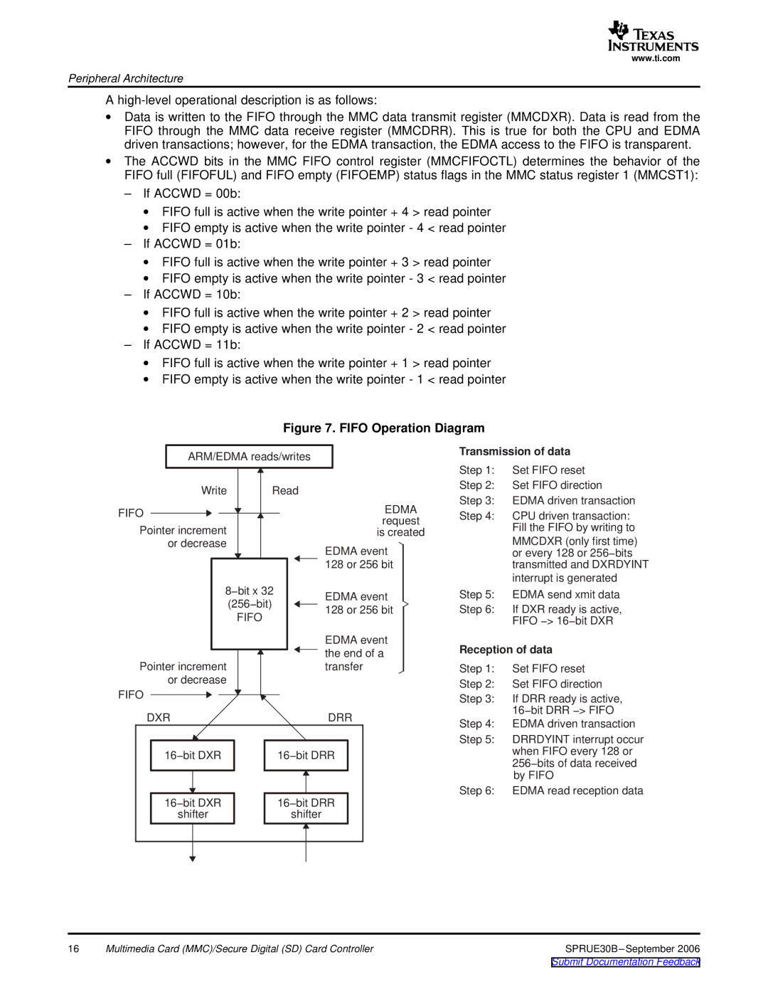
| Figure 7. FIFO Operation Diagram |
| ||
ARM/EDMA reads/writes |
| Transmission of data | ||
|
|
| ||
|
|
| Step 1: | Set FIFO reset |
Write | Read |
| Step 2: | Set FIFO direction |
| Step 3: | EDMA driven transaction | ||
|
| EDMA | ||
FIFO |
| Step 4: | CPU driven transaction: | |
| request | |||
Pointer increment |
|
| Fill the FIFO by writing to | |
| is created |
| ||
or decrease |
| EDMA event |
| MMCDXR (only first time) |
|
|
| or every 128 or 256−bits | |
|
| 128 or 256 bit |
| transmitted and DXRDYINT |
|
|
| interrupt is generated |
8−bit x 32 |
| EDMA event | Step 5: EDMA send xmit data |
(256−bit) |
| ||
| 128 or 256 bit | Step 6: If DXR ready is active, | |
FIFO |
| ||
|
| FIFO −> 16−bit DXR | |
|
|
|
| EDMA event | Reception of data | ||
| the end of a | |||
|
|
| ||
Pointer increment | transfer | Step 1: | Set FIFO reset | |
or decrease |
| Step 2: | Set FIFO direction | |
FIFO |
| |||
| Step 3: | If DRR ready is active, | ||
|
| |||
DXR | DRR |
| 16−bit DRR −> FIFO | |
Step 4: | EDMA driven transaction | |||
|
| |||
|
| Step 5: | DRRDYINT interrupt occur | |
16−bit DXR | 16−bit DRR |
| when FIFO every 128 or | |
| 256−bits of data received | |||
|
|
| ||
|
|
| by FIFO | |
16−bit DXR | 16−bit DRR | Step 6: | EDMA read reception data | |
|
| |||
shifter | shifter |
|
| |
16 | Multimedia Card (MMC)/Secure Digital (SD) Card Controller | SPRUE30B |