www.ti.com
Registers
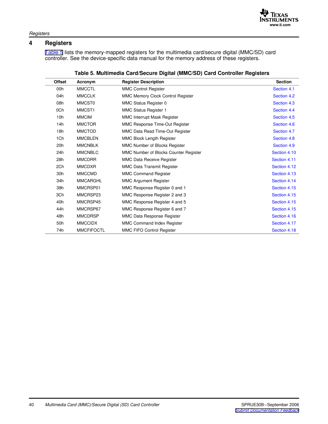
4Registers
Table 5 lists the
Table 5. Multimedia Card/Secure Digital (MMC/SD) Card Controller Registers
Offset | Acronym | Register Description | Section |
00h | MMCCTL | MMC Control Register | Section 4.1 |
04h | MMCCLK | MMC Memory Clock Control Register | Section 4.2 |
08h | MMCST0 | MMC Status Register 0 | Section 4.3 |
0Ch | MMCST1 | MMC Status Register 1 | Section 4.4 |
10h | MMCIM | MMC Interrupt Mask Register | Section 4.5 |
14h | MMCTOR | MMC Response | Section 4.6 |
18h | MMCTOD | MMC Data Read | Section 4.7 |
1Ch | MMCBLEN | MMC Block Length Register | Section 4.8 |
20h | MMCNBLK | MMC Number of Blocks Register | Section 4.9 |
24h | MMCNBLC | MMC Number of Blocks Counter Register | Section 4.10 |
28h | MMCDRR | MMC Data Receive Register | Section 4.11 |
2Ch | MMCDXR | MMC Data Transmit Register | Section 4.12 |
30h | MMCCMD | MMC Command Register | Section 4.13 |
34h | MMCARGHL | MMC Argument Register | Section 4.14 |
38h | MMCRSP01 | MMC Response Register 0 and 1 | Section 4.15 |
3Ch | MMCRSP23 | MMC Response Register 2 and 3 | Section 4.15 |
40h | MMCRSP45 | MMC Response Register 4 and 5 | Section 4.15 |
44h | MMCRSP67 | MMC Response Register 6 and 7 | Section 4.15 |
48h | MMCDRSP | MMC Data Response Register | Section 4.16 |
50h | MMCCIDX | MMC Command Index Register | Section 4.17 |
74h | MMCFIFOCTL | MMC FIFO Control Register | Section 4.18 |
40 | Multimedia Card (MMC)/Secure Digital (SD) Card Controller | SPRUE30B |
|
| Submit Documentation Feedback |