Texas Instruments TMS320DM644x Data Flow in the Input/Output Fifo, MMC/SD Mode Read Sequence, Crc

Models: TMS320DM644x

1 61
Download 61 pages 29.83 Kb
Page 15
Image 15

www.ti.com

Peripheral Architecture

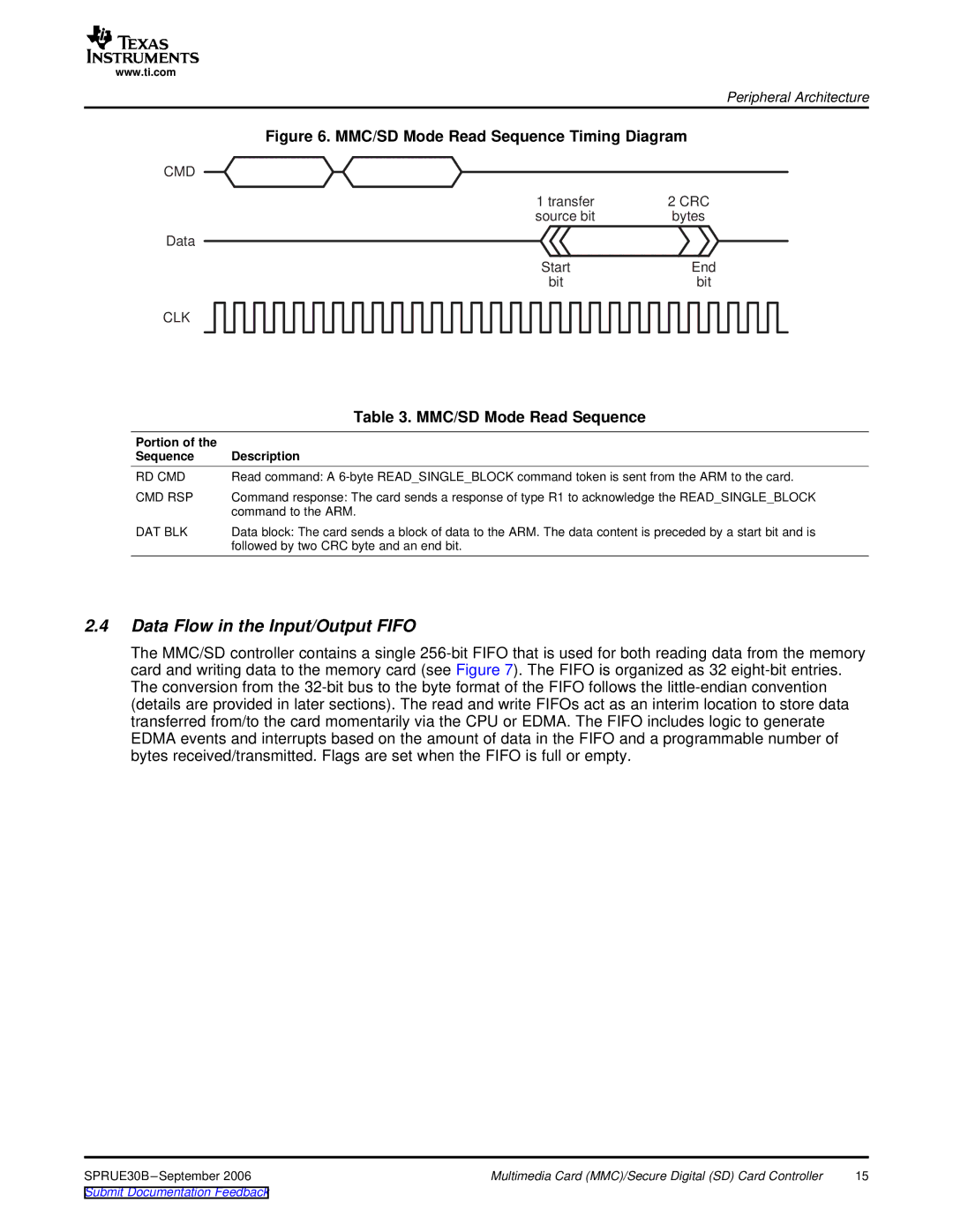
Figure 6. MMC/SD Mode Read Sequence Timing Diagram

CMD


1 transfer

2 CRC

source bit

bytes

Data


Start

End

bit

bit

CLK


Table 3. MMC/SD Mode Read Sequence

Portion of the


Sequence

Description

RD CMD

Read command: A 6-byte READ_SINGLE_BLOCK command token is sent from the ARM to the card.

CMD RSP

Command response: The card sends a response of type R1 to acknowledge the READ_SINGLE_BLOCK


command to the ARM.

DAT BLK

Data block: The card sends a block of data to the ARM. The data content is preceded by a start bit and is


followed by two CRC byte and an end bit.

2.4Data Flow in the Input/Output FIFO

The MMC/SD controller contains a single 256-bit FIFO that is used for both reading data from the memory card and writing data to the memory card (see Figure 7). The FIFO is organized as 32 eight-bit entries. The conversion from the 32-bit bus to the byte format of the FIFO follows the little-endian convention (details are provided in later sections). The read and write FIFOs act as an interim location to store data transferred from/to the card momentarily via the CPU or EDMA. The FIFO includes logic to generate EDMA events and interrupts based on the amount of data in the FIFO and a programmable number of bytes received/transmitted. Flags are set when the FIFO is full or empty.

SPRUE30B –September 2006

Multimedia Card (MMC)/Secure Digital (SD) Card Controller

15

Submit Documentation Feedback

Page 15
Image 15
Texas Instruments TMS320DM644x manual Data Flow in the Input/Output Fifo, MMC/SD Mode Read Sequence, Crc, Rd Cmd