R
Chapter 3: Family Specific Considerations
bitstream is in use. When this occurs, external circuitry is responsible for re-initializing the FPGA and loading an alternate bitstream. This requires storage for two complete bitstreams and another device, such as a CPLD, for managing the reconfiguration process. The reconfiguration process cannot be controlled by the FPGA because the FPGA becomes inactive during configuration.
The bitstream loaded in response to RTR will become active after the bus reset and the design will not be present to observe the busmode and buswidth broadcast. Missing the busmode broadcast is not an issue, as the newly loaded bitstream will be correct for the busmode in use. However, the newly loaded bitstream will not know if the bus is 32-bit or 64-bit. Upon the assertion of RTR, the FPGA must save the buswidth state in the CPLD so that the CPLD can restore it later.
Bus width is visible on the PCIW_EN signal when the Buswidth Detect Disable option is set to false in the CFG module, even if previously set to true. Buswidth may be forced by setting this option to true and then setting Bus Width Manual As 32-bit appropriately. While single bitstream designs will set these CFG options to permanent true or false values, it is possible to control these options dynamically by adding ports to the CFG module and making signal assignments to CFG[502] and CFG[503]. This important concern is a board level design requirement and the exact implementation is dependent on the specific configuration method used. For more information about saving these values and designing a mechanism to reconfigure the FPGA, see XAPP 938.
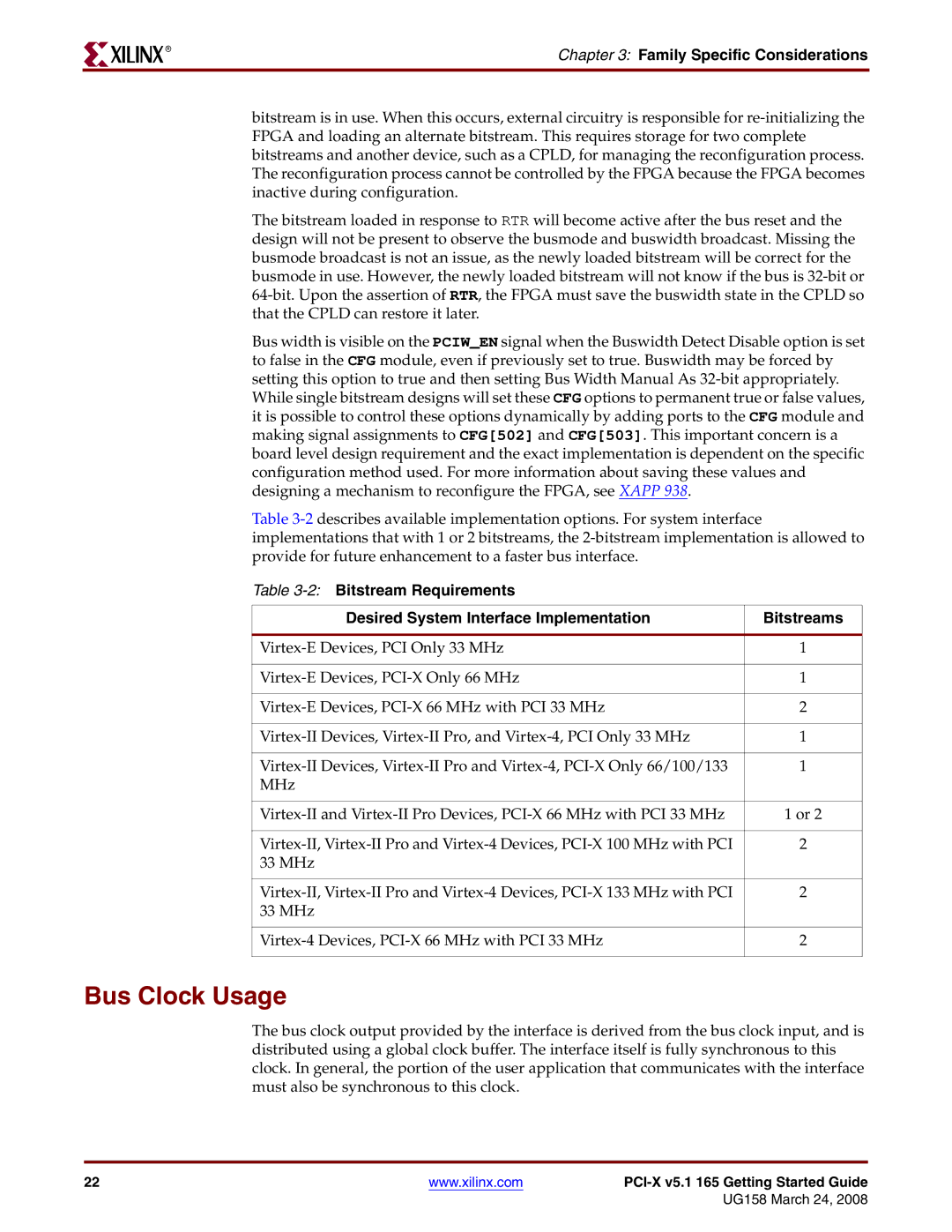
Table 3-2describes available implementation options. For system interface implementations that with 1 or 2 bitstreams, the 2-bitstream implementation is allowed to provide for future enhancement to a faster bus interface.
Table 3-2:Bitstream Requirements
Desired System Interface Implementation | Bitstreams |
| |
Virtex-E Devices, PCI Only 33 MHz | 1 |
| |
Virtex-E Devices, PCI-X Only 66 MHz | 1 |
| |
Virtex-E Devices, PCI-X 66 MHz with PCI 33 MHz | 2 |
| |
Virtex-II Devices, Virtex-II Pro, and Virtex-4, PCI Only 33 MHz | 1 |
| |
Virtex-II Devices, Virtex-II Pro and Virtex-4, PCI-X Only 66/100/133 | 1 |
MHz | |
| |
Virtex-II and Virtex-II Pro Devices, PCI-X 66 MHz with PCI 33 MHz | 1 or 2 |
| |
Virtex-II, Virtex-II Pro and Virtex-4 Devices, PCI-X 100 MHz with PCI | 2 |
33 MHz | |
| |
Virtex-II, Virtex-II Pro and Virtex-4 Devices, PCI-X 133 MHz with PCI | 2 |
33 MHz | |
| |
Virtex-4 Devices, PCI-X 66 MHz with PCI 33 MHz | 2 |
| |
Bus Clock Usage
The bus clock output provided by the interface is derived from the bus clock input, and is distributed using a global clock buffer. The interface itself is fully synchronous to this clock. In general, the portion of the user application that communicates with the interface must also be synchronous to this clock.
22 | www.xilinx.com | PCI-X v5.1 165 Getting Started Guide |
| | UG158 March 24, 2008 |