Electrical Compliance
R
It is important to note that the frequency of this clock is not guaranteed to be constant. In fact, in a compliant system, the clock may be any frequency, up to and including the maximum allowed frequency, and the frequency may change on a
For these reasons, the user application should not use this clock as an input to a DLL or PLL, nor should the user application use this clock in the design of interval timers (for example, DRAM refresh counters).
Electrical Compliance
The
Although the core interface provides a direct PME# output from a general purpose I/O pin, this output signal has certain limitations. If the FPGA power is removed, the general purpose I/O pin will appear as a low impedance to ground. This appears to the system as an assertion of PME#. For this reason, implementations that use the PME# signal should employ an external buffering scheme that will prevent false assertions of PME# when power is removed from the FPGA device.
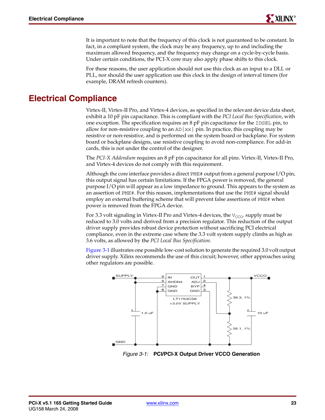
For 3.3 volt signaling in
driver supply provides robust device protection without sacrificing PCI electrical compliance, even in the extreme case where the 3.3 volt system supply climbs as high as
3.6volts, as allowed by the PCI Local Bus Specification.
Figure 3-1 illustrates one possible low-cost solution to generate the required 3.0 volt output driver supply. Xilinx recommends the use of this circuit; however, other approaches using other regulators are possible.
SUPPLY8
5
7
6
INOUT
SHDN# ADJ
GNDBYP
GND GND
LT1763CS8
+3.0V SUPPLY
1
2
4
3
VCCO
38.3, 1%
1.0uF
10uF
26.1, 1%
GND
Figure 3-1: PCI/PCI-X Output Driver VCCO Generation
| www.xilinx.com | 23 |
UG158 March 24, 2008