Chapter 1: SP601 Evaluation Board
Figure 1-8 provides the UCF constraints for the SPI serial flash PROM.
NET "FPGA_D2_MISO3" | LOC = "V14"; |
NET "SPI_CS_B" | LOC = "V3"; |
NET "FPGA_D0_DIN_MISO_MISO1" | LOC = "R13"; |
NET "FPGA_D1_MISO2" | LOC = "T14"; |
NET "FPGA_MOSI_CSI_B_MISO0" | LOC = "T13"; |
NET "FPGA_CCLK" | LOC = "R15"; |
Figure 1-8: UCF Location Constraints for BPI Flash Connections
References
See the Winbond Serial Flash specifications for more information at http://www.winbond-
usa.com/hq/enu/ProductAndSales/ProductLines/FlashMemory/SerialFlash/W25X64.htm.
See the XPS Serial Peripheral Interface specification for more information at http://www.xilinx.com/support/documentation/ip_documentation/xps_spi.pdf.
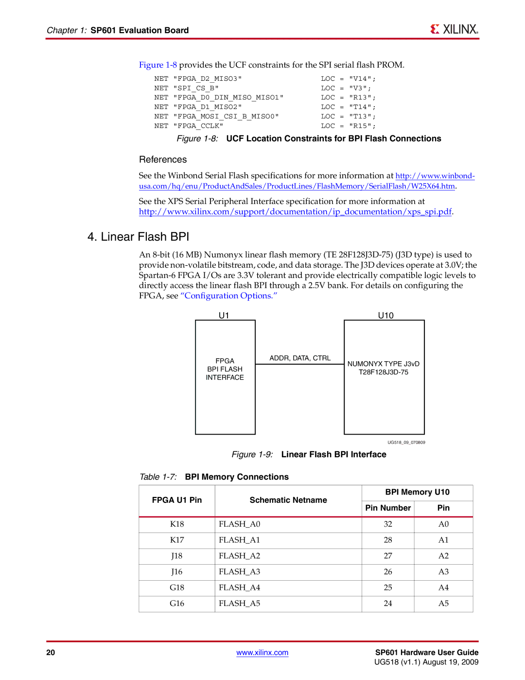
4. Linear Flash BPI
An
U1 | U10 |
FPGA
BPI FLASH INTERFACE
ADDR, DATA, CTRL
NUMONYX TYPE J3vD
UG518_09_070809
Figure 1-9: Linear Flash BPI Interface
Table 1-7: BPI Memory Connections
FPGA U1 Pin | Schematic Netname | BPI Memory U10 | ||
|
| |||
Pin Number | Pin | |||
|
| |||
|
|
|
| |
K18 | FLASH_A0 | 32 | A0 | |
|
|
|
| |
K17 | FLASH_A1 | 28 | A1 | |
|
|
|
| |
J18 | FLASH_A2 | 27 | A2 | |
|
|
|
| |
J16 | FLASH_A3 | 26 | A3 | |
|
|
|
| |
G18 | FLASH_A4 | 25 | A4 | |
|
|
|
| |
G16 | FLASH_A5 | 24 | A5 | |
|
|
|
| |
20 | www.xilinx.com | SP601 Hardware User Guide |
|
| UG518 (v1.1) August 19, 2009 |