Detailed Description
8-Kb NV Memory
The SP601 hosts a
Table
FPGA U1 Pin | Schematic Netname | SPI Memory U7 | |||
|
| ||||
Number |
|
| |||
Pin Number | Pin | ||||
|
| ||||
|
|
| |||
|
|
|
|
| |
Not Applicable | Tied to GND |
| 1 | A0 | |
|
|
|
|
| |
Not Applicable | Tied to GND |
| 2 | A1 | |
|
|
|
| ||
Not Applicable | Pulled up (0 ohm) to VCC3V3 | 3 | A2 | ||
|
|
|
|
| |
N10 | IIC_SDA_MAIN |
| 5 | SDA | |
|
|
|
|
| |
P11 | IIC_SCL_MAIN |
| 6 | SCL | |
|
|
|
|
| |
Not Applicable | Tied to GND |
| 7 | WP | |
|
|
|
|
| |
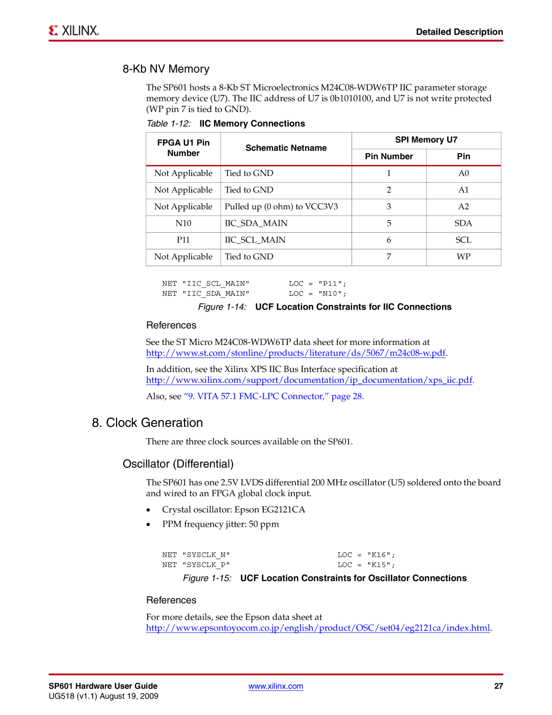
NET "IIC_SCL_MAIN" | LOC = "P11"; |
|
| ||
NET "IIC_SDA_MAIN" | LOC = "N10"; |
|
| ||
Figure 1-14: UCF Location Constraints for IIC Connections
References
See the ST Micro
In addition, see the Xilinx XPS IIC Bus Interface specification at
http://www.xilinx.com/support/documentation/ip_documentation/xps_iic.pdf.
Also, see “9. VITA 57.1
8. Clock Generation
There are three clock sources available on the SP601.
Oscillator (Differential)
The SP601 has one 2.5V LVDS differential 200 MHz oscillator (U5) soldered onto the board and wired to an FPGA global clock input.
•Crystal oscillator: Epson EG2121CA
•PPM frequency jitter: 50 ppm
NET | "SYSCLK_N" | LOC | = | "K16"; |
NET | "SYSCLK_P" | LOC | = | "K15"; |
Figure 1-15: UCF Location Constraints for Oscillator Connections
References
For more details, see the Epson data sheet at http://www.epsontoyocom.co.jp/english/product/OSC/set04/eg2121ca/index.html.
SP601 Hardware User Guide | www.xilinx.com | 27 |
UG518 (v1.1) August 19, 2009