Chapter 1: SP601 Evaluation Board
Configuration Options
The FPGA on the SP601 Evaluation Board can be configured by the following methods:
•“3. SPI x4 Flash,” page 18
•“4. Linear Flash BPI,” page 20
•“JTAG Configuration,” page 42
For more information, refer to the
Table
Mode Pins (M1, M0) | Configuration Mode |
|
|
00 | Master Byte Peripheral Interface (BPI) |
|
|
01 | Master SPI x1, x2, or x4 |
|
|
10 | Not implemented on SP601 |
|
|
11 | Not implemented on SP601 |
|
|
JTAG Configuration
JTAG configuration is provided through onboard
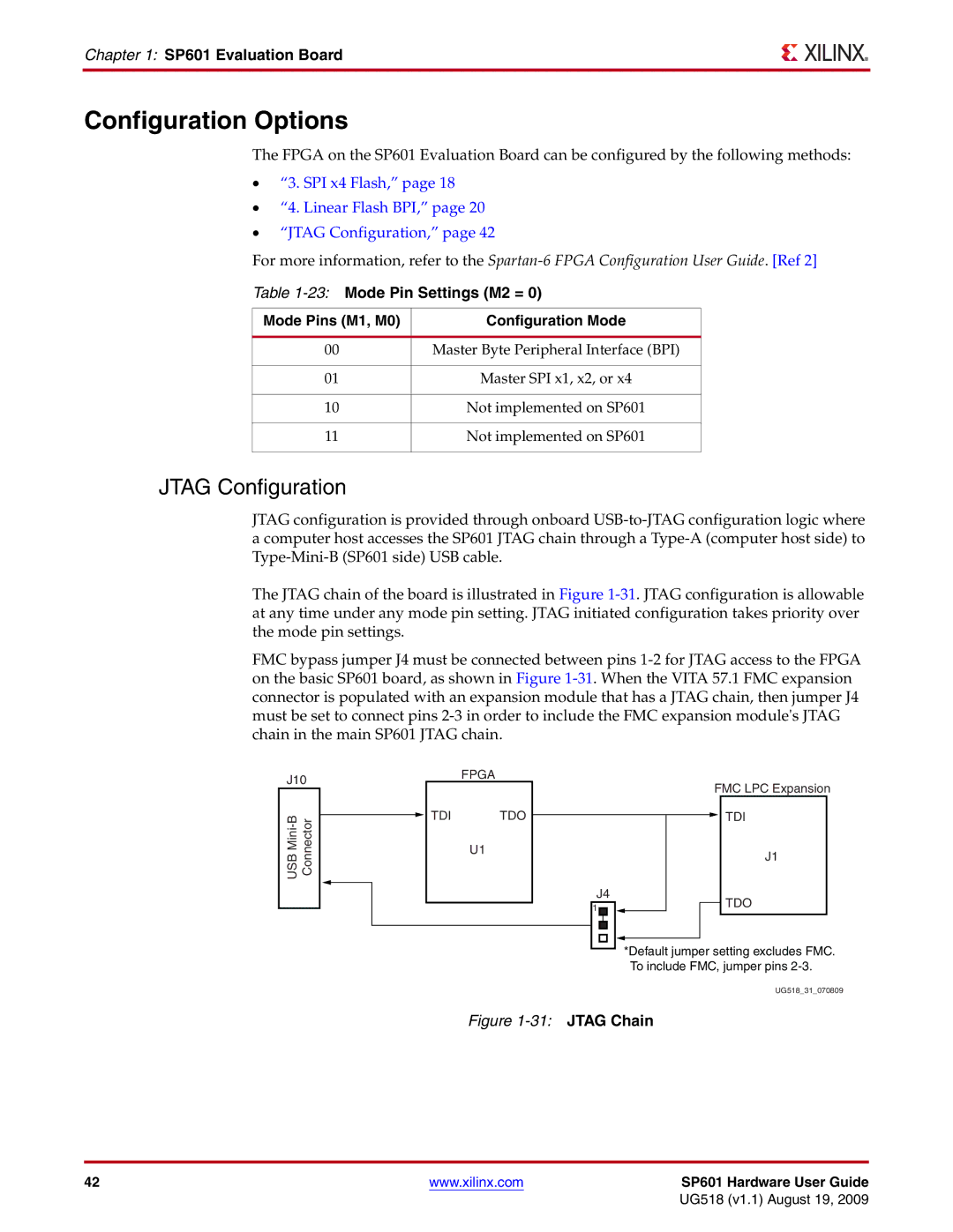
The JTAG chain of the board is illustrated in Figure
FMC bypass jumper J4 must be connected between pins
J10
USB
FPGA
![]() TDI TDO
TDI TDO
U1
J4
1 ![]()
![]()
FMC LPC Expansion
![]() TDI
TDI
J1
TDO
*Default jumper setting excludes FMC. To include FMC, jumper pins
UG518_31_070809
Figure 1-31: JTAG Chain
42 | www.xilinx.com | SP601 Hardware User Guide |
|
| UG518 (v1.1) August 19, 2009 |