Chapter 1: SP601 Evaluation Board
3. SPI x4 Flash
The Xilinx Spartan-6 FPGA hosts a SPI interface which is visible to the Xilinx iMPACT configuration tool. The SPI memory device operates at 3.0V; the Spartan-6 FPGA I/Os are 3.3V tolerant and provide electrically compatible logic levels to directly access the SPI flash through a 2.5V bank. The XC6SLX16-2CSG324 is a master device when accessing an external SPI flash memory device.
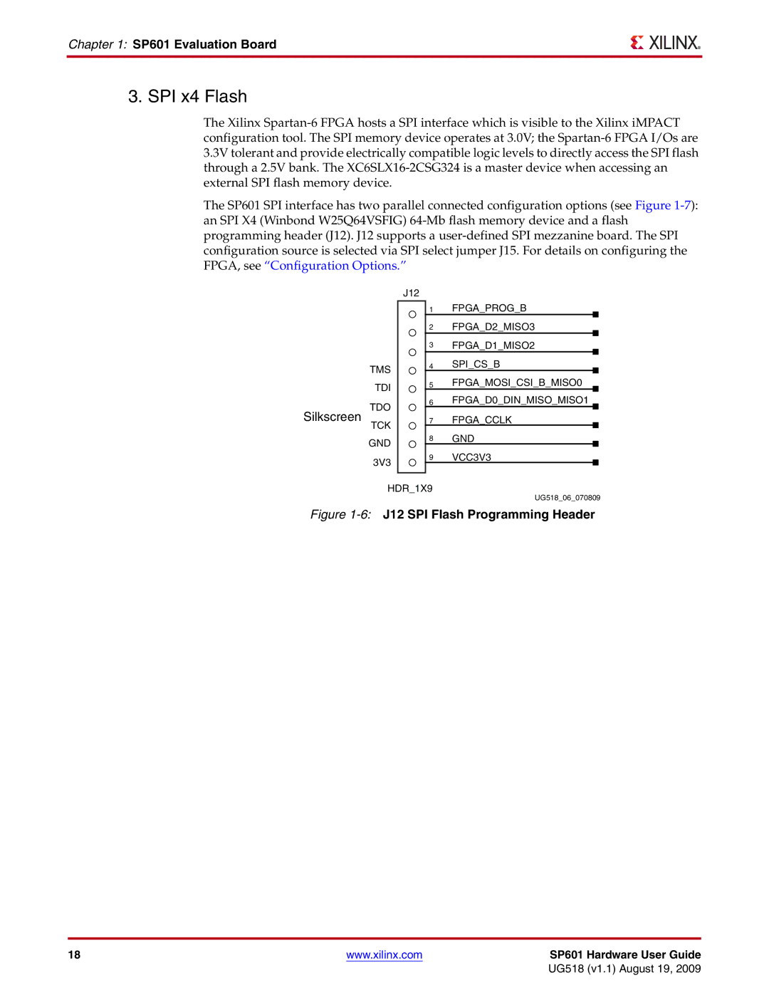
The SP601 SPI interface has two parallel connected configuration options (see Figure 1-7): an SPI X4 (Winbond W25Q64VSFIG) 64-Mb flash memory device and a flash programming header (J12). J12 supports a user-defined SPI mezzanine board. The SPI configuration source is selected via SPI select jumper J15. For details on configuring the FPGA, see “Configuration Options.”
TMS
TDI
TDO
Silkscreen
TCK
GND 3V3
J12
1FPGA_PROG_B
2FPGA_D2_MISO3
3FPGA_D1_MISO2
4SPI_CS_B
5FPGA_MOSI_CSI_B_MISO0
6FPGA_D0_DIN_MISO_MISO1
7FPGA_CCLK
8GND
9VCC3V3
HDR_1X9
UG518_06_070809
Figure 1-6:J12 SPI Flash Programming Header
18 | www.xilinx.com | SP601 Hardware User Guide |
| | UG518 (v1.1) August 19, 2009 |