Related Xilinx Documents
Block Diagram
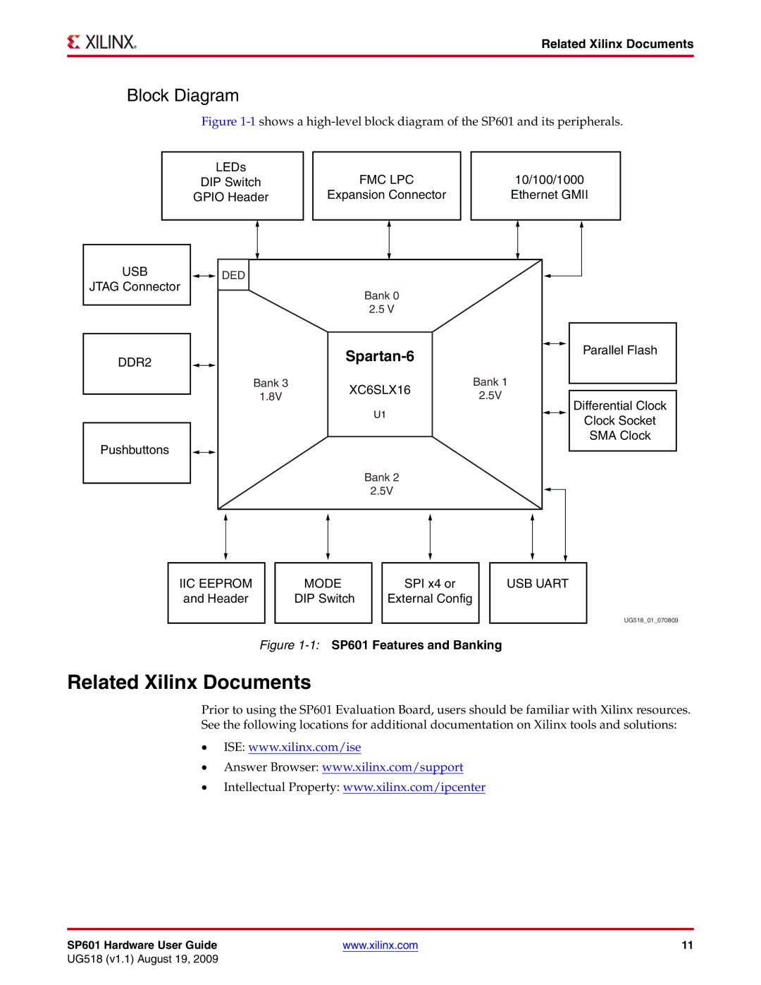
Figure 1-1 shows a high-level block diagram of the SP601 and its peripherals.
LEDs
DIP Switch
GPIO Header
FMC LPC
Expansion Connector
10/100/1000
Ethernet GMII
USB
JTAG Connector
DDR2
Pushbuttons
DED |
|
| |
| Bank 0 |
| |
| 2.5 V |
| |
|
|
| |
Bank 3 | XC6SLX16 | Bank 1 | |
1.8V | 2.5V | ||
| |||
| U1 |
| |
| Bank 2 |
| |
| 2.5V |
|
Parallel Flash
Differential Clock
Clock Socket
SMA Clock
IIC EEPROM |
| MODE |
| SPI x4 or |
| USB UART |
and Header |
| DIP Switch |
| External Config |
|
|
|
|
|
|
|
|
|
Figure 1-1: SP601 Features and Banking
UG518_01_070809
Related Xilinx Documents
Prior to using the SP601 Evaluation Board, users should be familiar with Xilinx resources. See the following locations for additional documentation on Xilinx tools and solutions:
•ISE: www.xilinx.com/ise
•Answer Browser: www.xilinx.com/support
•Intellectual Property: www.xilinx.com/ipcenter
SP601 Hardware User Guide | www.xilinx.com | 11 |
UG518 (v1.1) August 19, 2009