SCSI BUS
01 | G | 02 | |
|
|
|
|
03 | G | 04 | |
|
|
|
|
05 | G | 06 | |
|
|
|
|
07 | G | 08 | |
|
|
|
|
09 | G | 10 | |
|
|
|
|
11 | G | 12 | |
|
|
|
|
13 | G | 14 | |
|
|
|
|
15 | G | 16 | |
|
|
|
|
17 | G | 18 | |
|
|
|
|
19 | G | G | 20 |
|
|
|
|
21 | G | G | 22 |
|
|
|
|
23 | G | G | 24 |
|
|
|
|
25 | Open | TERMPWR* | 26 |
|
|
|
|
27 | G | G | 28 |
|
|
|
|
29 | G | G | 30 |
|
|
|
|
31 | G | 32 | |
|
|
|
|
33 | G | G | 34 |
|
|
|
|
35 | G | 36 | |
|
|
|
|
37 | G | 38 | |
|
|
|
|
39 | G | 40 | |
|
|
|
|
41 | G |
| 42 |
|
|
|
|
43 | G |
| 44 |
|
|
|
|
45 | G | 46 | |
|
|
|
|
47 | G | 48 | |
|
|
|
|
49 | G | 50 | |
|
|
|
|
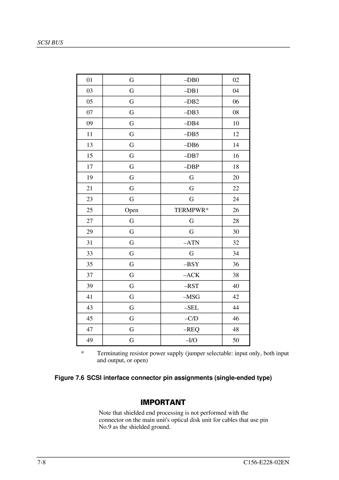
*Terminating resistor power supply (jumper selectable: input only, both input and output, or open)
Figure 7.6 SCSI interface connector pin assignments (single-ended type)
Note that shielded end processing is not performed with the connector on the main unit's optical disk unit for cables that use pin No.9 as the shielded ground.
