Design Checklist

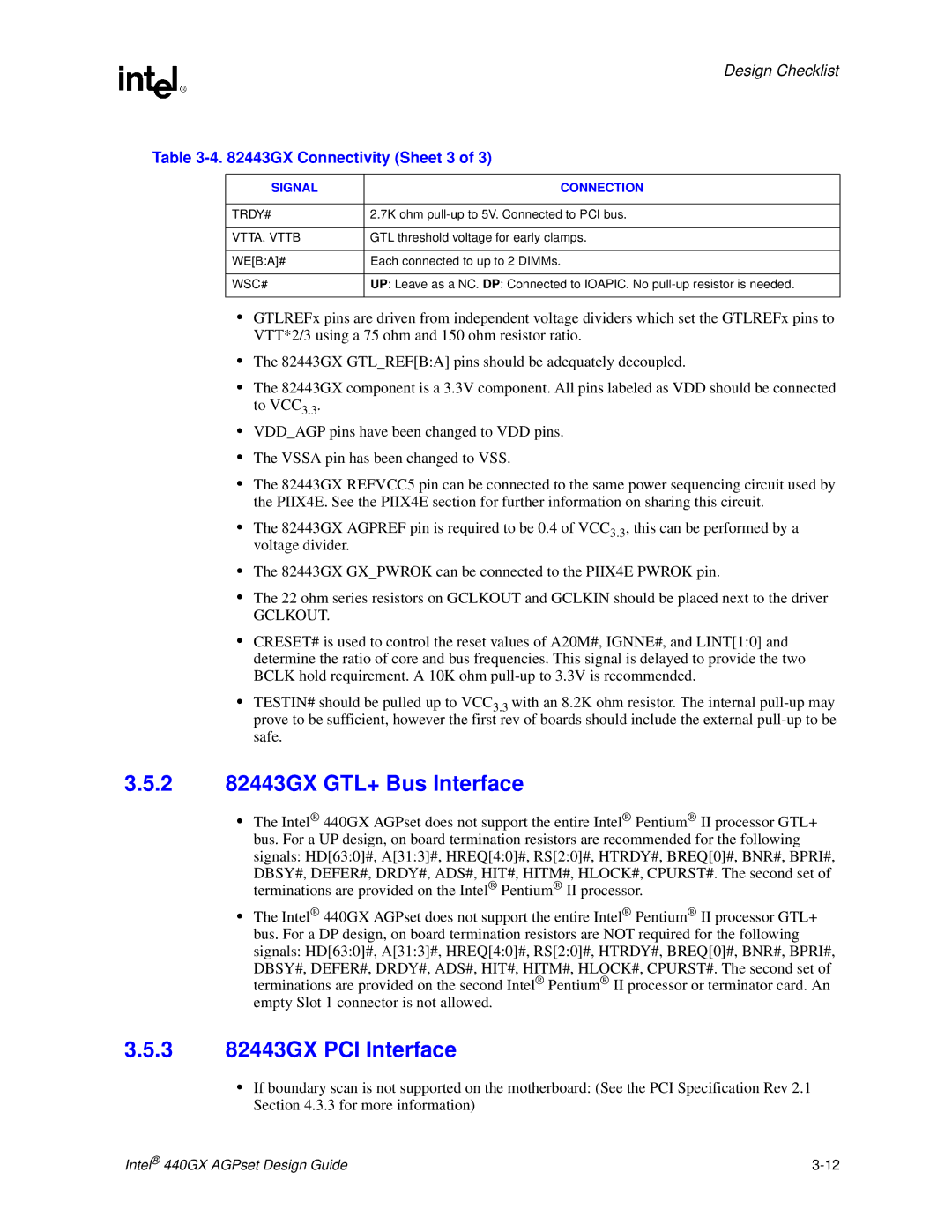
Table 3-4. 82443GX Connectivity (Sheet 3 of 3)

SIGNAL

CONNECTION


TRDY#

2.7K ohm pull-up to 5V. Connected to PCI bus.


VTTA, VTTB

GTL threshold voltage for early clamps.


WE[B:A]#

Each connected to up to 2 DIMMs.


WSC#

UP: Leave as a NC. DP: Connected to IOAPIC. No pull-up resistor is needed.


GTLREFx pins are driven from independent voltage dividers which set the GTLREFx pins to VTT*2/3 using a 75 ohm and 150 ohm resistor ratio.

The 82443GX GTL_REF[B:A] pins should be adequately decoupled.

The 82443GX component is a 3.3V component. All pins labeled as VDD should be connected to VCC3.3.

VDD_AGP pins have been changed to VDD pins.

The VSSA pin has been changed to VSS.

The 82443GX REFVCC5 pin can be connected to the same power sequencing circuit used by the PIIX4E. See the PIIX4E section for further information on sharing this circuit.

The 82443GX AGPREF pin is required to be 0.4 of VCC3.3, this can be performed by a voltage divider.

The 82443GX GX_PWROK can be connected to the PIIX4E PWROK pin.

The 22 ohm series resistors on GCLKOUT and GCLKIN should be placed next to the driver

GCLKOUT.

CRESET# is used to control the reset values of A20M#, IGNNE#, and LINT[1:0] and determine the ratio of core and bus frequencies. This signal is delayed to provide the two BCLK hold requirement. A 10K ohm pull-up to 3.3V is recommended.

TESTIN# should be pulled up to VCC3.3 with an 8.2K ohm resistor. The internal pull-up may prove to be sufficient, however the first rev of boards should include the external pull-up to be safe.

3.5.282443GX GTL+ Bus Interface

The Intel® 440GX AGPset does not support the entire Intel® Pentium® II processor GTL+ bus. For a UP design, on board termination resistors are recommended for the following signals: HD[63:0]#, A[31:3]#, HREQ[4:0]#, RS[2:0]#, HTRDY#, BREQ[0]#, BNR#, BPRI#,

DBSY#, DEFER#, DRDY#, ADS#, HIT#, HITM#, HLOCK#, CPURST#. The second set of terminations are provided on the Intel® Pentium® II processor.

The Intel® 440GX AGPset does not support the entire Intel® Pentium® II processor GTL+ bus. For a DP design, on board termination resistors are NOT required for the following signals: HD[63:0]#, A[31:3]#, HREQ[4:0]#, RS[2:0]#, HTRDY#, BREQ[0]#, BNR#, BPRI#,

DBSY#, DEFER#, DRDY#, ADS#, HIT#, HITM#, HLOCK#, CPURST#. The second set of terminations are provided on the second Intel® Pentium® II processor or terminator card. An empty Slot 1 connector is not allowed.

3.5.382443GX PCI Interface

If boundary scan is not supported on the motherboard: (See the PCI Specification Rev 2.1 Section 4.3.3 for more information)

Intel®440GX AGPset Design Guide

3-12

Page 72
Image 72
Intel 440GX manual 2 82443GX GTL+ Bus Interface, 3 82443GX PCI Interface, GX Connectivity Sheet 3, VTTA, Vttb, Wsc#

440GX specifications

The Intel 440GX chipset was launched in 1997 as part of Intel's series of chipsets known as the 440 family, and it served as a critical component for various Pentium II and Pentium III-based motherboard architectures. Specifically designed for the second generation of Intel’s processors, the 440GX delivered enhanced performance and supported a range of important technologies that defined PC architectures of its time.

One of the main features of the Intel 440GX was its support for a 100 MHz front-side bus (FSB), which significantly improved data transfer rates between the CPU and the memory subsystem. This advancement allowed the 440GX to accommodate both the original Pentium II processors as well as the later Pentium III chips, providing compatibility and flexibility for system builders and consumers alike.

The 440GX chipset included an integrated AGP (Accelerated Graphics Port) controller, which supported AGP 2x speeds. This enabled high-performance graphics cards to be utilized effectively, delivering many enhanced graphics capabilities for gaming and multimedia applications. The AGP interface was crucial at the time as it offered a dedicated pathway for graphics data, increasing bandwidth compared to traditional PCI slots.

In terms of memory support, the 440GX could address up to 512 MB of SDRAM, allowing systems built with this chipset to run comfortably with sufficient memory for the era’s demanding applications. The memory controller was capable of supporting both single and double-sided DIMMs, which provided versatility in memory configuration for system builders.

Another notable feature of the Intel 440GX was its support for multi-processor configurations through its Dual Processors support feature. This allowed enterprise and workstation computers to leverage the performance advantages of multiple CPUs, making the chipset suitable for business and professional environments where multitasking and high-performance computing were essential.

On the connectivity front, the chipset supported up to six PCI slots, enhancing peripheral device integration and expansion capabilities. It also included integrated IDE controllers, facilitating connections for hard drives and CD-ROM devices.

Overall, the Intel 440GX chipset represented a balanced combination of performance, flexibility, and technology advancements for its time. Its introduction helped establish a foundation for subsequent advancements in PC technology and set the stage for more powerful computing systems in the years to come.