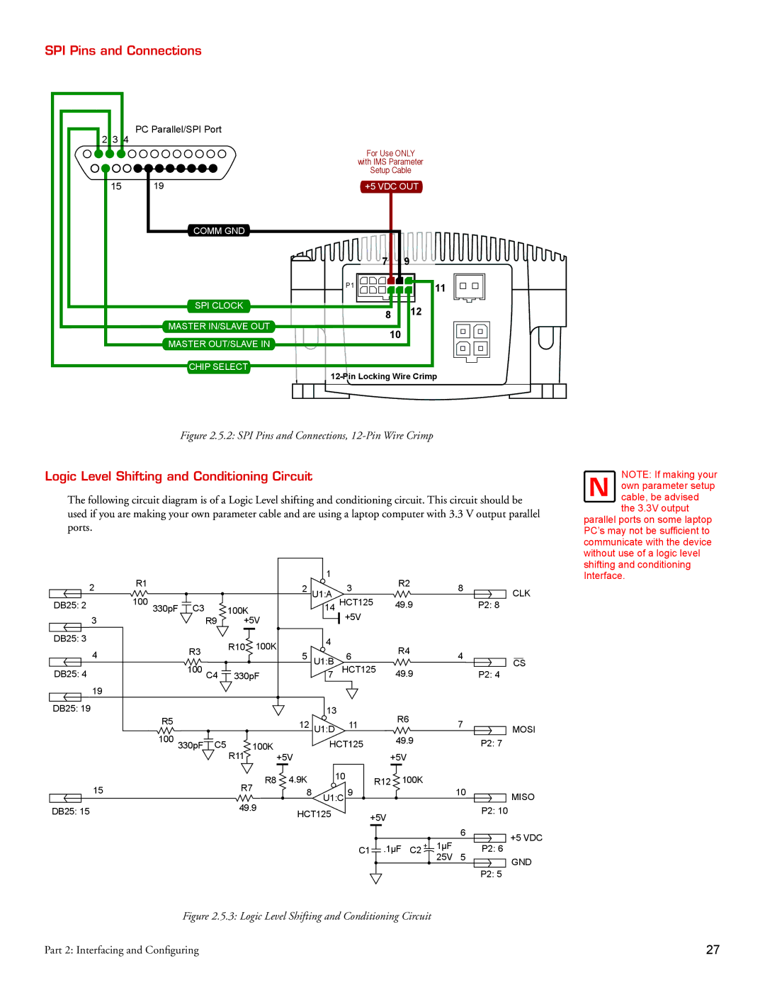
SPI Pins and Connections
PC Parallel/SPI Port
2 3 4
For Use ONLY
with IMS Parameter
Setup Cable
15 | 19 | +5 VDC OUT |
COMM GND
7 | 9 |
P1 | 11 |
|
SPI CLOCK | 8 | 12 |
|
MASTER IN/SLAVE OUT MASTER OUT/SLAVE IN
CHIP SELECT
10
Figure 2.5.2: SPI Pins and Connections, 12-Pin Wire Crimp
Logic Level Shifting and Conditioning Circuit
The following circuit diagram is of a Logic Level shifting and conditioning circuit. This circuit should be used if you are making your own parameter cable and are using a laptop computer with 3.3 V output parallel ports.
| R1 |
|
|
|
|
|
|
| 1 |
|
| R2 |
|
|
| |
2 |
|
|
|
|
|
| 2 | U1:A | 3 |
|
| 8 | CLK | |||
100 330pF |
|
|
|
|
|
|
|
|
| |||||||
DB25: 2 | C3 |
| 100K |
|
|
| 14 | HCT125 | 49.9 |
|
| P2: 8 | ||||
3 |
|
|
| R9 | +5V |
|
|
| +5V |
|
|
|
|
|
| |
|
|
|
|
|
|
|
|
|
|
|
|
| ||||
DB25: 3 |
|
|
|
| R10 | 100K |
| 4 |
|
|
|
|
|
|
| |
|
|
| R3 |
|
|
|
| R4 |
|
|
| |||||
4 |
|
|
| 5 |
| 6 |
|
| 4 |
| ||||||
|
|
|
|
|
| U1:B |
|
| CS | |||||||
|
|
|
|
|
|
|
|
|
|
| ||||||
|
|
| 100 C4 |
|
|
|
|
|
|
| ||||||
DB25: 4 |
|
| 330pF |
|
| 7 | HCT125 | 49.9 |
|
| P2: 4 | |||||
19 |
|
|
|
|
|
|
|
|
|
|
|
|
|
|
|
|
DB25: 19 | R5 |
|
|
|
|
|
|
| 13 |
| R6 |
|
|
| ||
|
|
|
|
|
|
| 12 | U1:D | 11 |
|
| 7 | MOSI | |||
| 100 |
|
|
|
|
|
|
| 49.9 |
| ||||||
| 330pF | C5 |
| 100K |
| HCT125 |
|
|
| P2: 7 | ||||||
|
| R11 | +5V |
| +5V |
|
| |||||||||
|
|
|
|
|
|
|
|
|
|
|
|
| ||||
|
|
|
|
| R7 | R8 | 4.9K |
| 10 | R12 | 100K |
|
|
| ||
15 |
|
|
|
| U1:C 9 |
| 10 |
| ||||||||
|
|
|
|
| 8 |
|
|
|
| MISO | ||||||
|
|
|
|
| 49.9 |
|
|
|
|
| ||||||
DB25: 15 |
|
|
|
|
| HCT125 |
| +5V |
|
|
| P2: 10 | ||||
|
|
|
|
|
|
|
|
|
|
| ||||||
|
|
|
|
|
|
|
|
|
|
|
|
|
|
| ||
|
|
|
|
|
|
|
|
|
|
|
|
|
|
| 6 | +5 VDC |
|
|
|
|
|
|
|
|
|
|
|
|
| C2 + | 1µF |
| |
|
|
|
|
|
|
|
|
|
| C1 |
| .1µF | 5 | P2: 6 | ||
|
|
|
|
|
|
|
|
|
|
|
|
|
| 25V | GND | |
|
|
|
|
|
|
|
|
|
|
|
|
|
|
|
| |
|
|
|
|
|
|
|
|
|
|
|
|
|
|
|
| P2: 5 |
NOTE: If making your own parameter setup cable, be advised the 3.3V output
parallel ports on some laptop PC’s may not be sufficient to communicate with the device without use of a logic level shifting and conditioning Interface.
Figure 2.5.3: Logic Level Shifting and Conditioning Circuit
Part 2: Interfacing and Configuring | 27 |