Page
Rabbit 3000 Microprocessor
Rabbit Semiconductor
Trademarks
Table of Contents
Rabbit Internal I/O Registers
Parallel Ports 129
Rabbit 3000 Clocks 209
Appendix B. Rabbit 3000 Revisions 273
Rabbit 3000 Microprocessor
Introduction
Features and Specifications Rabbit
User’s Manual
1shows a block diagram of the Rabbit
CPU
Summary of Rabbit 3000 Advantages
Differences Rabbit 3000 vs. Rabbit
Feature Rabbit
Serial ports with support for SDLC/HDLC IrDA
Rabbit 3000 Design Features
Rabbit 8-bit Processor vs. Other Processors
Serial Ports
Overview of On-Chip Peripherals and Features
1 5 V Tolerant Inputs
4 32.768 kHz Oscillator Input
System Clock
Cascaded Output Registers for Parallel Ports D and E
Parallel I/O
Rabbit
Slave Port
Auxiliary I/O Bus
Timers
PWM
Input Capture Channels
Pulse Width Modulation Outputs
Quadrature Encoder Inputs
Programming Port
Separate Core and I/O Power Pins
Design Standards
Spread Spectrum Clock
Dynamic C Support for the Rabbit
Standard Bios
Rabbit 3000 Microprocessor
Processor Registers
Details on Rabbit Microprocessor Features
Rabbit 3000 Microprocessor
Addressing Memory Components
Memory Mapping
Example of Memory Mapping Operation
4shows a memory interface unit
Extended Code Space
Use of XPC Segment
Separate I and D Space Extending Data Memory
Xpc window stack
Using the Stack Segment for Data Storage
Data RAM Root Code
Practical Memory Considerations
User’s Manual
Instruction Set Outline
Load or Store Data from or to a Constant Address
Load Immediate Data to a Register
Other 8-bit loads and stores are the following
Load or Store Data Using an Index Register
Register Exchanges
Register-to-Register Move
7 16-bit Arithmetic and Logical Ops
Push and Pop Instructions
Bool
SBC instruction can also be used to perform a sign extension
Input/Output Instructions
Manipulation of Boolean Variables
How to Do It in Assembly Language-Tips and Tricks
Zero HL in 4 Clocks
Exchanges Not Directly Implemented
Comparisons of Integers
HLB
Atomic Moves from Memory to I/O Space
Interrupt Priority
Interrupt Structure
Processor Priority Effect on Interrupts
Effect of Processor Priorities on Interrupts
Privileged Instructions, Critical Sections and Semaphores
Multiple External Interrupting Devices
Critical Sections
Semaphores Using Bit B,HL
Computed Long Calls and Jumps
Precisely Timed Output Pulses
Rabbit Capabilities
Pulse Width Modulation to Reduce Relay Power
Open-Drain Outputs Used for Key Scan
Using Open-Drain Outputs for Key Scan
Cold Boot
Slave Port
Slave Rabbit As a Protocol Uart
PIN Assignments and Functions
Pinout
Lqfp Package
Same pin dimensions apply along the x axis and the y axis
Mechanical Dimensions and Land Pattern
PC Board Land Pattern for Rabbit 3000 128-pin Lqfp
Ball Grid Array Package
C D E F G H J K L M
Nominal Ball Tolerance Ball Pitch Nominal Land
Ball and Land Size Dimensions
Design Considerations All dimensions in mm
Key Feature Recommendation
BGA Package Outline
Lqfp Tfbga
Rabbit Pin Descriptions
Rabbit Pin Descriptions
Pin Pin Group Pin Name Direction Function Numbers
Vddcore
Bus Timing Read and Write
Bus Timing
Pins With Alternate Functions
Description of Pins with Alternate Functions
PF7 PWM3 AQD2A
Parallel Port x Alternate Functions Control Bits
Parallel Port x Alternate Functions
Symbol Parameter Test Conditions Min Typ Max Units
DC Characteristics
3 Volt DC Characteristics
Symbol Parameter Maximum Rating
I/O Buffer Sourcing and Sinking Limit
Rabbit 3000 Microprocessor
Rabbit Internal I/O Registers
On-Chip Peripheral ISR Starting Address
Rabbit 3000 Peripherals and Interrupt Service Vectors
Rabbit Internal I/O Registers
Default Values for all the Peripheral Control Registers
Register Name Mnemonic Address Reset
Grev
PEB7R
PWM0R
Tbcsr
Sdar
Processor Identification
Global ROM Configuration Register
Global RAM Configuration Register
Miscellaneous Functions
Gcpu
Rabbit Oscillators and Clocks
Global CPU Register
Global Revision Register
Rabbit
Gcsr
Global Control/Status Register
Clock Select Field of Gcsr
Global Control/Status Register
Gcdr
Recommended Delays Set In Gcdr for Clock Doubler
Clock Doubler
Global Clock Double Register
Effect of Clock Doubler
User’s Manual
Reduction in Peak Spectral Strength from Spectrum Spreader
Clock Spectrum Spreader
Chip Select Options for Low Power
Address = 0x0D
Global Power Save Control Register
Short Chip Select Memory Read
Global Output Control Register Gocr = 0x0E
Output Pins CLK, STATUS, /WDTOUT, /BUFEN
Time/Date Clock Real-Time Clock
11. Real-Time Clock Control Register Rtccr adr =
10. Real-Time Clock RTCxR Data Registers
12. Watchdog Timer Control Register Wdtcr adr =
Watchdog Timer
13. Watchdog Timer Test Register Wdttr adr =
System Reset
Pin Name Direction Reset Low Post-Reset† Recognized by CPU
14. Rabbit 3000 Reset Sequence and State of I/O Pins
Rabbit Interrupt Structure
15. Interrupts-Priority and Action to Clear Requests
External Interrupt Line Logic
External Interrupts
Reg Name Reg Address Bits 7,6 Bits 5,4 Bits 3,2 Bits 1,0
Interrupt Vectors INT0 EIR,0x00/INT1 EIR,0x08
16. Control Registers for External Interrupts
Bootstrap Operation
102 Rabbit 3000 Microprocessor
Pulse Width LSBs 1st 2nd 3rd 4th
Pulse Width Modulator
18. PWM MSB x Register
17. PWM LSB x Register
Input Capture
106 Rabbit 3000 Microprocessor
Iccsr
19. Input Capture Control/Status Register
Input Capture Control/Status Register
ICT1R
20. Input Capture Control Register
21. Input Capture Trigger x Register
Iccr
24. Input Capture MSB x Register
22. Input Capture Source x Register
23. Input Capture LSB x Register
Quadrature Decoder
Rejected
Qdcsr
25. Quadrature Decoder Control/Status Register
Quad Decode Control/Status Register
QDC1R
26. Quadrature Decoder Control Register
27. Quadrature Decoder Count Register
Qdcr
114 Rabbit 3000 Microprocessor
Interface for Static Memory Chips
Memory Interface and Mapping
RAM
Rabbit
Data Lines Static Address Lines Memory Flash
Processor Memory Mapping Unit Interface Memory Chips
Memory Mapping Overview
Memory-Mapping Unit
Segment Register Function
64K
Segment Registers
Segment Size Register
Memory Interface Unit
Memory Bank Control Register x MBxCR = 0x014 +
Memory Bank Control Registers
Mmidr
Optional A16, A19 Inversions by Segment /CS1 Enable
MMU Instruction/Data Register Mmidr =
MMU Instruction/Data Register
Memory Timing Control Register
Memory Timing Control Register MTCR, adr =
MMU Expanded Code Register
Mecr
Bdcr
Allocation of Extended Code and Data
Breakpoint/Debug Control Register BDCR, adr = 0x01C
Breakpoint/Debug Control Register
Instruction and Data Space Support
RAM
Use of Physical Memory Separate I & D Space Model
How the Compiler Compiles to Memory
128 Rabbit 3000 Microprocessor
Parallel Ports
Parallel Port a Data Register Bit Functions
Parallel Port a
Parallel Port a Registers
Parallel Port B Register Bit Functions
Parallel Port B
Parallel Port B Registers
Parallel Port C Register Bit Functions
Parallel Port C
Parallel Port C Registers
Parallel Port D Registers
Parallel Port D
PD7
Bits 7 Bits 5 Bits 3 Bits 1
Parallel Port D Register functions
Parallel Port D Control Register adr =
136 Rabbit 3000 Microprocessor
PE0
Parallel Port E
10. Parallel Port E Registers
12. Parallel Port E Control Register adr =
11. Parallel Port E Register functions
14. Parallel Port F Register Functions
Parallel Port F
13. Parallel Port F Registers
15. Parallel Port F Control Register adr = 0x03C
Using Parallel Port a and Parallel Port F
Summary Parallel Port a Parallel Port F
17. Parallel Port G Data Register Functions
Parallel Port G
16. Parallel Port G Registers
Parallel Port G Control Register adr= 0x04C
External I/O Timing with 1 wait state
10. I/O Bank Control Registers
Write data Write strobe T1 Tw T2
Read data Read strobe Chip select strobe
I/O Bank x Control Register
Control Register Port E Address Pin A1513 Range
External I/O Register Address Range and Pin Mapping
148 Rabbit 3000 Microprocessor
Timers
Reload Register Operation
Timer a
Timer a I/O Registers
Timer a I/O Registers
Tacsr
Timer a Capabilities
Timer a Control and Status Register
User’s Manual 153
Tapr
Timer a Control Register
Timer a Prescale Register
Tacr
Practical Use of Timer a
Register Name Mnemonic Reset Address
Timer B
Timer B Registers
Tbcr
Timer B Control and Status Register
Timer B Control Register
Tbcsr
12. Timer B Count LSB Register
Timer B Count MSB x Registers
10. Timer B Count LSB x Registers
11. Timer B Count MSB Register
Using Timer B
160 Rabbit 3000 Microprocessor
Rabbit Serial Ports
Serial Port Signals
Serial Port Signal Name Function
Clka
User’s Manual 163
Serial Port Register Layout
Signals Shown at Microprocessor Tx Pin
User’s Manual 165
Serial Port C Registers
Serial Port Registers
Serial Port a Registers
Serial Port B Registers
Serial Port F Registers
Serial Port D Registers
Serial Port E Registers
Address Register All Ports
Data Register All Ports
10. Long Stop Register All Ports
11. Status Register Asynchronous Mode Only All Ports
12. Status Register Clocked Serial Ports A-D only
Bits Value Description Clocked serial mode only
Bits Value Description Hdlc mode only
13. Status Register Hdlc Mode Ports E and F only
Sbcr
14. Serial Port Control Register Ports a and B
Sacr
Sdcr
15. Serial Port Control Register Ports C and D
Sccr
Address = 0xE4
Sfcr
16. Serial Port Control Register Ports E and F
Secr
Address = 0xCC
17. Extended Register Asynchronous Mode All Ports
18. Extended Register Clocked Serial Mode Ports A-D only
19. Extended Register Hdlc Mode Ports E and F only
Transmitter IRQ
Serial Port Interrupt
Transmit Serial Data Timing
Serial Port Synchronization
Receive Serial Data Timing
Clocked Serial Ports
Clock Polarities Supported in Clocked Serial Mode
User’s Manual 183
184 Rabbit 3000 Microprocessor
Clocked Serial Timing with External Clock
Clocked Serial Timing
Clocked Serial Timing With Internal Clock
Valid
Synchronous Communications on Ports E and F
Last Byte Bit Pattern Valid Data Hits
User’s Manual 189
190 Rabbit 3000 Microprocessor
User’s Manual 191
Push AF IOI LD A,SCSR
Serial Port Software Suggestions
Transmitting Dummy Characters
Controlling an RS-485 Driver and Receiver
Transmitting and Detecting a Break
Using a Serial Port to Generate a Periodic Interrupt
Stop bit
Parity, Extra Stop Bits with 7-Data-Bit Characters
Parity, Extra Stop Bits with 8-Data-Bit Characters
Stop bit Start bit Data bits 9th bit low
Data Framing/Modbus
Supporting 9th Bit Communication Protocols
Rabbit-Only Master/Slave Protocol
User’s Manual 197
198 Rabbit 3000 Microprocessor
SRD SCS
Rabbit Slave Port
Slave Port Read Cycle
Following table explains the parameters used in Figure
Symbol Parameter Minimum Maximum
Slaveattn PB7
Typical Connection Slave Rabbit to Master Rabbit
Register Mnemonic Internal Address External Address
Hardware Design of Slave Port Interconnection
Slave Port Registers
Slave Port Registers
Bit Bits 6,5 Bit 3,2 Bits 1,0 Write Only Read Only
Slave Port Control Register Spcr adr =
Slave Port Status Register Spsr adr =
Applications and Communications Protocols for Slaves
Slave Applications
Master-Slave Messaging Protocol
208 Rabbit 3000 Microprocessor
Rabbit 3000 Main Oscillator Circuit
Rabbit 3000 Clocks
Low-Power Design
EMI Control
Using the Clock Spectrum Spreader
Power Supply Connections and Board Layout
GCM1R
Spread Spectrum Enable/Disable Register
Spread Spectrum Mode Select
GCM0R
214 Rabbit 3000 Microprocessor
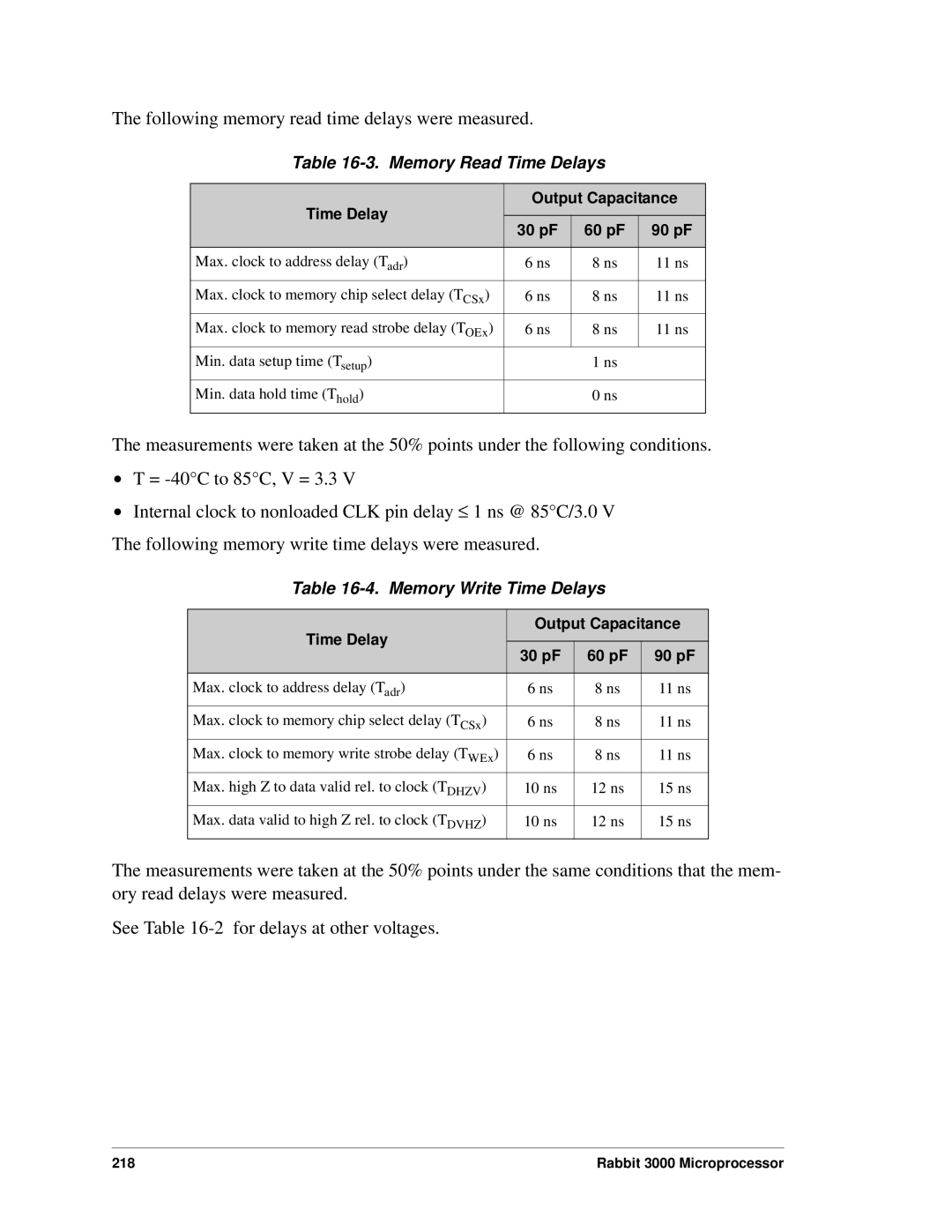
Memory Requirements at 3.3 V, -40C to +85C, Adr Bus 60 pF
AC Timing Specifications
Memory Access Time
Access Enable Access MHz
Normal Strong 30 pF 60 pF 90 pF No dbl/dbl
Data and Clock Delays VDD ±10%, Temp, -40C-+85C maximum
VDD
CSx
Time Delay Output Capacitance 30 pF 60 pF 90 pF
Memory Read Time Delays
Memory Write Time Delays
CLK A190 CSx WEx D70
Example
Clock Doubler Max-Min Clock Low Times
222 Rabbit 3000 Microprocessor
Bufen
16.2 I/O Access Time
I/O Write Time Delays
I/O Read Time Delays
Further Discussion of Bus and Clock Timing
Clock Doubler and Memory Timing
Period Frequency
Maximum Clock Speeds
Maximum Clock Speeds at 3.3 V Preliminary
Conditions Commercial Ratings Industrial Ratings
External Oscillator Buffer
User’s Manual 229
Power and Current Consumption
Rabbit 3000 System Current vs. Frequency at 3.3
11. Sleepy Mode Current Consumption
Current Consumption Mechanisms
Sleepy Mode Current Consumption
Memory Current Consumption
Current is negligible for V 1.14
Battery-Backed Clock Current Consumption
Voltage Current incl built-in buffer
Reduced-Power External Main Oscillator
Bios Services
Rabbit Bios and Virtual Driver
Bios
Periodic Interrupt
Bios Assumptions
Watchdog Timer Support
Virtual Driver
User’s Manual 239
240 Rabbit 3000 Microprocessor
Other Rabbit Software
Power Management Support
Reading and Writing I/O Registers
Using Assembly Language
Using Library Functions
Atomic Instruction
Shadow Registers
Updating Shadow Registers
Interrupt While Updating Registers
Non-atomic Instructions
Timer and Clock Usage
Write-only Registers Without Shadow Registers
Format of the structure used is the following
246 Rabbit 3000 Microprocessor
Summary
Rabbit Instructions
Flag Description
Spreadsheet Conventions
Rabbit Z180 Meaning
Symbols
19.4 16-bit Indexed Loads and Stores
Load Immediate Data
Load & Store to Immediate Address
19.3 8-bit Indexed Load and Store
Register to Register Moves
19.5 16-bit Load and Store 20-bit Address
19.9 16-bit Arithmetic and Logical Ops
Exchange Instructions
Stack Manipulation Instructions
ADD A,HL
19.10 8-bit Arithmetic and Logical Ops
19.12 8-bit Increment and Decrement
19.11 8-bit Bit Set, Reset and Test
19.14 8-bit Shifts and Rotates
19.13 8-bit Fast a Register Operations
Block Move Instructions
Instruction Prefixes
Miscellaneous Instructions
Control Instructions Jumps and Calls
Following instructions are privileged
Privileged Instructions
Differences Rabbit VS. Z80/Z180 Instructions
Z80/Z180 Instructions Dropped Rabbit Instructions to Use
Flag Register Key
IOI and IOE I Column Symbol Key
Rabbit Z180 Meaning
Z V C
EX AF,AF
LD A,BC
LDP HL,IX
RRA
268 Rabbit 3000 Microprocessor
Programming Port PIN Assignments
Appendix A. the Rabbit Programming Port
Alternate Programming Port
Use of the Programming Port as a Diagnostic/Setup Port
Suggested Rabbit Crystal Frequencies
Non-Stock Crystals
Appendix B. Rabbit 3000 Revisions
274 Rabbit 3000 Microprocessor
User’s Manual 275
IL1T/IZ1T IL2T/IZ2T
Discussion of Fixes and Improvements
Table B-1. Summary of Rabbit 3000 Improvements and Fixes
Rabbit Description 3000 3000A
Rabbit Internal I/O Registers
Table B-2. Reset State of New Rabbit 3000A I/O Registers
Iuer
Rabbit Register Name Mnemonic 3000 3000A Address Reset
On-Chip Peripheral Address Range ISR Starting Address
Peripheral and ISR Address
User’s Manual 281
Gcpu Grev
Revision-Level ID Register
Table B-5. Rabbit 3000 Revision Identification Information
Processor Revision Package
System/User Mode
Wpcr
Memory Protection
Table B-6. Write Protect Control Register
Write Protect Control Register
Wplr
Table B-7. Write Protect Low Register
Write Protect Low Register
Wpsar
Table B-8. Write Protect High Register
Table B-9. Write Protect Segment x Register
Wphr
Wpsblr
Table B-10. Write Protect Segment x Low Register
Write Protect Segment x Low Register
Wpsalr
Wpsbhr
Table B-11. Write Protect Segment x High Register
Write Protect Segment x High Register
Wpsahr
Figure B-2. Simple Stack Protection Layout
Stack Protection
Table B-14. Stack High Limit Register
Table B-12. Stack Limit Control Register
Table B-13. Stack Low Limit Register
Ramsr
RAM Segment Relocation
Table B-15. RAM Segment Register
RAM Segment Register
Wdtcr
Secondary Watchdog Timer
Table B-16. Watchdog Timer Control Register-Updated
Table B-17. Secondary Watchdog Timer Register
New UMA/UMS Opcodes
New Opcodes
Table B-18. New Rabbit 3000 Opcodes
Instruction Bytes Clks Operation
IOI/IOE
Table B-19. Rabbit 3000 Revision Block Copy Opcode Effects
New Block Copy Opcodes
Source Destination
Table B-20. MMU Instruction/Data Register
Expanded I/O Memory Addressing
Table B-21 Bank x Control Register
External I/O Improvements
Address = 0x000D
Table B-22. Global Power Save Control Register
Short Chip Select Timing for Writes
Table B-24. Clock Select Field of Gcsr
Clock Select and Power Save Modes
Table B-23. Global Control/Status Register
Figure B-3. Short Chip Select Timing CLK/8, Read Operation
Short Chip Select Timing
Figure B-4. Short Chip Select Timing CLK/6, Read Operation
Figure B-6. Short Chip Select Timing CLK/2, Read Operation
Figure B-7. Short Chip Select Timing 2 kHz, Read Operation
Figure B-9. Short Chip Select Timing 8 kHz, Read Operation
Figure B-11. Short Chip Select Timing 32 kHz, Read Operation
Figure B-12. Short Chip Select Timing CLK/8, Write Operation
Figure B-13. Short Chip Select Timing CLK/6, Write Operation
Figure B-15. Short Chip Select Timing CLK/2, Write Operation
Figure B-16. Short Chip Select Timing 2 kHz, Write Operation
Figure B-18. Short Chip Select Timing 8 kHz, Write Operation
310 Rabbit 3000 Microprocessor
Figure B-21. PWM Interrupt and Output Timing
Pulse Width Modulator Improvements
PWM LSB 1 Register
Table B-25. PWM LSB 0 Register
Table B-26. PWM LSB 1 Register
PWM LSB 0 Register
Address = 0x008E
Table B-27. PWM LSB 2 and 3 Registers
Address = 0x008C
QDC1HR
Quadrature Decoder Improvements
Table B-28. Quadrature Decoder Control Register
Table B-29. Quadrature Decoder Count High Register
User’s Manual 315
Serial Ports E/F
Pins with Alternate Functions
Table C-1. Differences Between System and User Modes
Appendix C. SYSTEM/USER Mode
System Mode User Mode
Instruction Bytes Clk Operation Priv
System/User Mode Opcodes
Table C-2. New System/User Mode Opcodes
Table C-3. System/User Mode I/O Registers
System/User Mode Registers
Register Name Mnemonic Address
Table C-4. I/O Addresses Inaccessible in User Mode
Interrupts
Figure C-1. Interrupt Handing in System/User Mode
Peripheral Interrupt Prioritization
Table C-5. Interrupts-Priority and Action to Clear Requests
Memory Protection Only
Using the System/User Mode
Figure C-3. System/User Mode Setup for Mixed Operation
Mixed System/User Mode Operation
Complete Operating System
Figure C-4. System/User Mode Setup for Operating System
Table D-1 Rabbit 3000A Internal I/O Registers
Appendix D. Rabbit 3000A Internal I/O Registers
Table D-1. Rabbit 3000A Internal I/O Registers
0x03C0 00000000 Serial Port E User Enable Register
0x006A Xxxxxxxx Port D Bit 3 Register
0x0082 00000000 Bank 3 Control Register
0x0098 Xx000000 Interrupt 1 Control Register
0x00D1 Xxxxxxxx Serial Port B Long Stop Register
334 Rabbit 3000 Microprocessor
User’s Manual 335
Page
Numerics
Index
Memory A16, A19 inversions /CS1
PWL2R, PWL3R
200