88F6281
Hardware Specifications
Document Conventions Document Status
88F6281 Hardware Specifications
Doc Status Preliminary Technical Publication
88F6281
Hardware Specifications
Integrated Controller
High-performance CPU core, running at up to
Features
Supports Ieee 802.1Qav draft Audio Video Bridging networks
Features
Bit/4-bit SDmem, SDIO, and MMC cards Up to 50 MHz
GbE Port 0 in Gmii mode or GbE Port
TDM
X16
Table of Contents
132
Table of Contents
129
130
Clocking
List of Tables
List of Tables
88F6281 Part Order Options 132
Hsbga 288-pin Package Dimensions 131
Revision History 134
List of Figures
Pin and Signal Descriptions
Inter-IC Sound I2S Test Circuit 107
Related Documentation
About this Document
Preface
Following conventions are used in this document
Document Conventions
Pin and Signal Descriptions
Misc PCI Express
Power
Pin Logic
Flash
Term Definition
Pin Descriptions
Pin Functions and Assignments Table Key
Interface Pin Prefix Codes
SPI Sdio TDM PTP
88F6281 Hardware Specifications Interface Pin Prefix Codes
RTC
MPP Twsi Uart
Power Pin Assignments
Power Supply Pins
Pin Name Description Type
88F6281 Hardware Specifications Power Pin Assignments
Miscellaneous Pin Assignment
Pin Name Power Description Type Rail
Miscellaneous Pin Assignments
Mcke Sstl Vddm
DDR Sdram Interface Pin Assignments
DDR Sdram Interface Pin Assignments
Mclkout Sstl Vddm
Mncal
Mstartburst Sstl Vddm
Mstart Sstl Vddm
Burstin Mpcal
PCI Express Interface Pin Assignments
PCI Express Interface Pin Assignments
Sata Interface Pin Assignments
Pin Name Power Rail Description Type
Sata Port Interface Pin Assignment
Gigabit Ethernet Port Interface Pin Assignments
Pin Name Type Power Rail Description
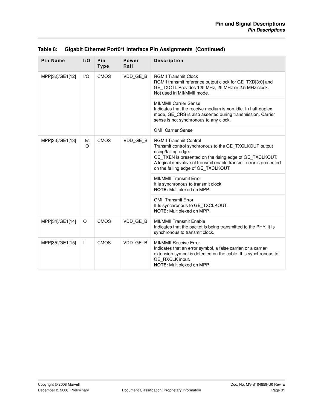
Gigabit Ethernet Port0/1 Interface Pin Assignments
Gerxclk Cmos Vddgea
Gerxctl Cmos Vddgea
Cmos Vddgeb
To any clock
Gmii Receive Error
MPP2724
MII/MMII Collision Detect
MPP32/GE112
MII/MMII Transmit Error
Gmii Transmit Error
MII/MMII Receive Error
Gemdio Cmos Vddgea
Serial Management Interface SMI Interface Pin Assignments
Serial Management Interface SMI Pin Assignments
Gemdc Cmos Vddgea
USB 2.0 Interface Pin Assignments
USB 2.0 Interface Pin Assignments
USB 2.0 Data Differential Pair
Jtag Pin Assignment
Jtag Interface Pin Assignment
Rtcxout
Real Time Clock RTC Interface Pin Assignments
RTC Interface Pin Assignments
Rtcxin
Nfale Cmos Vddo
Nand Flash Interface Pin Assignment
Nand Flash Interface Pin Assignment
Nfcle Cmos Vddo
MPP Interface Pin Assignment
MPP Interface Pin Assignment
Twsck Cmos Vddo
Two-Wire Serial Interface Twsi Interface
Two-Wire Serial Interface Twsi Interface Pin Assignment
Twsda Cmos Vddo
Uart Port 0/1 Interface Pin Assignment
Uart Interface
Fs is the audio sample rate
Audio S/PDIF / I2S Interface Signal Assignment
Audio S/PDIF / I2S Interface
Multiplexing option
SPICSn
Serial Peripheral Interface SPI Interface Signal Assignment
Pin Name Pin Type Power Rail Description
Serial Peripheral Interface SPI Interface
Sdclk Cmos Vddo
Secure Digital Input/Output Sdio Interface
Sdcmd Cmos Vddo
Time Division Multiplexing TDM Interface
Time Division Multiplexing TDM Interface Signal Assignment
Tdmspimiso Cmos Vddo
Tdmspimosi Cmos Vddo
Transport Stream TS Interface
Transport Stream TS Interface Signal Assignment
Cmos Vddo TS0DATA6 Vddgeb
TSMP7 Cmos Vddo
TSMP8 Cmos Vddo
TSMP9 Cmos Vddo
Ptpeventreq Cmos Vddo
Precise Timing Protocol PTP Interface Signal Assignment
Precise Timing Protocol PTP Interface
Ptpclk Cmos Vddo
Internal Pull-up and Pull-down Pins
Internal Pull-up and Pull-down Pins
Pin Name Pin Number Pull up/Pull down
Unused Interface Strapping
Unused Interface Strapping
Unused Interface Strapping
88F6281 pin list is provided as an Excel file attachment
88F6281 Pin Map and Pin List
Pin Multiplexing
Multi-Purpose Pins Functional Summary
Pin Multiplexing
Sata LEDs Audio Nand flash GbE
MPP Functionality
MPP190 MPP3520 MPP4936
Gpio
Sysrsto Spimosi
MPP Function Summary
MPP Function Summary
TSMP0 Tdmspi Auspdifi
Configuration, on
Ethernet Ports Pins Multiplexing
Gigabit Ethernet GbE Pins Multiplexing on MPP
MPP34 MII1TXEN out GE114 MPP35 MII1RXERR GE115
TS Port Pin Multiplexing
Tsmp TS Multiplexing Pins on MPP
Clock Type Description
Clocking
88F6281Clocks
Lists the clocks in the 88F6281
Ptpclk
Clocking 88F6281Clocks
Supported Clock Combinations
Sata PHY PLL
Spread Spectrum Clock Generator Sscg
88F6192, and 88F6281 Functional Specifications
System Power Up/Down and Reset Settings
System Power Up/Down and Reset Settings
Power-Up/Down Sequence Requirements
Power-Up Sequence Requirements
Power-Down Sequence Requirements
Hardware Reset
88F6281
SYSRSTn Duration Counter
Reset Out Signal
Power On Reset POR
May reset all settings to the factory default values
PCI Express Root Complex Reset
PCI Express Reset
Sheeva CPU TAP Controller Reset
Pins Sample Configuration
Pin Configuration Function
Reset Configuration
Than the third Tclk cycle after SYSRSTn de-assertion
0x0-0x3 = Reserved
MPP33 Cpuclk to DDR CLK Ratio
0x4 =
PCI Express Clock 100 MHz Differential Clock Configuration
Sscg Disable
= Enable
= Disable
Serial ROM Data Structure
88F6281 Hardware Specifications Reset Configuration
Pin Configuration Function MPP18 Reserved
Serial ROM Initialization
Serial ROM Initialization Operation
Boot Sequence
88F6281 Hardware Specifications
Jtag Interface
Jtag Interface
TAP Controller
Instruction Register
Idcode Register Map
Bypass Register
Jtag Scan Chain
ID Register
Absolute Maximum Ratings
Electrical Specifications Preliminary
Electrical Specifications Preliminary
Absolute Maximum Ratings
RTC interface
88F6281 Hardware Specifications Absolute Maximum Ratings
125 Case temperature
125 Storage temperature
MPP, TWSI, JTAG, SDIO, I 2S, SPI
Recommended Operating Conditions
Recommended Operating Conditions
Parameter Min Typ Max Units Comments
Internal clock inverter for crystal
Analog supply for RTC in Battery
Back-up mode
105 Junction Temperature
Thermal Power Dissipation
Thermal Power Dissipation
CPU @ 1000 MHz
Interface Symbol Test Conditions Max Units
Current Consumption
Current Consumption
General 3.3V Interface Cmos DC Electrical Specifications
DC Electrical Specifications
General 3.3V Cmos DC Electrical Specifications
Electrical Specifications
65*VDDIO
Rgmii 1.8V Interface Cmos DC Electrical Specifications
35*VDDIO Input high level
VIH
Sdram DDR2 Interface DC Electrical Specifications
Sdram DDR2 Interface DC Electrical Specifications
RTT
Following table Vddio means the Vddo power rail
Twsi Interface 3.3V DC Electrical Specifications
SPI Interface 3.3V DC Electrical Specifications
Following table, Vddio means the Vddo power rail
TDM Interface 3.3V DC Electrical Specifications
Reference Clock AC Timing Specifications
AC Electrical Specifications
Reference Clock AC Timing Specifications
Tclk
Description Symbol Min Max Units Tdmspi Output Clock
SMI Master Mode Reference Clock
Twsi Master Mode Reference Clock
Sdram DDR2 Interface AC Timing Table
MHz @ Description Symbol Min Max
Sdram DDR2 Interface AC Timing
Sdram DDR2 Interface AC Timing Table
Sdram DDR2 Interface Address Timing Table
MHz @ Description Symbol Min Max Units
Sdram DDR2 Clock Specifications
Sdram DDR2 Clock Specifications
Description Symbol Min Max Units
CLK
Sdram DDR2 Interface AC Timing Diagrams
Sdram DDR2 Interface Test Circuit
VTT
Control
Address
DQSn TDSI tDHI
Rgmii 10/100 AC Timing Table at
Reduced Gigabit Media Independent Interface Rgmii AC Timing
Rgmii AC Timing Table
Rgmii 10/100/1000 AC Timing Table at
Rgmii Test Circuit
Rgmii AC Timing Diagram
Gmii Test Circuit
125 MHz Description Symbol Min Max
Gigabit Media Independent Interface Gmii AC Timing
Gmii AC Timing Table
TLOW THIGH
Gmii AC Timing Diagrams
TSETUP Hold
VILmax
MII/MMII MAC Mode AC Timing Table
5.1 MII/MMII MAC Mode AC Timing Table
5.2 MII/MMII MAC Mode Test Circuit
5.3 MII/MMII MAC Mode AC Timing Diagrams
MII/MMII MAC Mode Input AC Timing Diagram
Serial Management Interface SMI AC Timing
SMI Master Mode AC Timing Table
SMI Master Mode Test Circuit
SMI Master Mode AC Timing Table
MDC
SMI Master Mode AC Timing Diagrams
Jtag Interface Test Circuit
30 MHz Description Symbol Min Max Units
Jtag Interface AC Timing
Jtag Interface AC Timing Table
Jtag Interface Output Delay AC Timing Diagram
Jtag Interface AC Timing Diagrams
Twsi Master AC Timing Table
Two-Wire Serial Interface Twsi AC Timing
100 kHz Description Symbol
Twsi AC Timing Table
Twsi Test Circuit
Twsi AC Timing Diagrams
9.1 S/PDIF AC Timing Table
Sony/Philips Digital Interconnect Format S/PDIF AC Timing
Pdif AC Timing Table
Pdif Test Circuit
9.2 S/PDIF Test Circuit
Inter-IC Sound I2S AC Timing Table
Inter-IC Sound Interface I2S AC Timing
Inter-IC Sound I2S AC Timing Table
Inter-IC Sound I2S Test Circuit
Inter-IC Sound I2S Output Delay AC Timing Diagram
Inter-IC Sound I2S AC Timing Diagrams
TDM Interface Test Circuit
192 MHz Description Symbol Min Max Units
Time Division Multiplexing TDM Interface AC Timing
TDM Interface AC Timing Table
Pclk DTX
TDM Interface Timing Diagrams
Pclk DRX
Description Symbol Min Max
SPI Master Mode AC Timing Table
SPI Master Mode Test Circuit
SPI Master Mode AC Timing Table
Data Out TDOVmin TDOVmax TCSB TCSA
SPI Master Mode Timing Diagrams
TCH tCL
Sclk
Secure Digital Input/Output Sdio Test Circuit
Sdio Host in High Speed Mode AC Timing Table
Secure Digital Input/Output Sdio Interface AC Timing
Secure Digital Input/Output Sdio AC Timing Table
Sdio Host in High Speed Mode Output AC Timing Diagram
Secure Digital Input/Output Sdio AC Timing Diagrams
Transport Stream Input Interface AC Timing Table
Transport Stream TS Interface AC Timing
Transport Stream Interface AC Timing Table
Transport Stream Output Interface AC Timing Table
Transport Stream Interface Test Circuit
Transport Stream Interface Timing Diagrams
Transport Stream Input Interface AC Timing Diagram
Differential Interface Reference Clock Characteristics
Differential Interface Electrical Characteristics
Clock frequency FCK 100.0
PCI Express Interface Spread Spectrum Requirements
Symbol Min Max Units
Fmod 33.0
PCI Express Interface Driver and Receiver Characteristics
PCI Express Interface Electrical Characteristics
PCI Express Interface Driver and Receiver Characteristics
PCI Express Interface Test Circuit
PCI Express Interface Test Circuit
Sata Interface Electrical Characteristics
Rlid
Rlod
TJ5
DJ5
18.0 Differential return loss 300 MHz-600 MHz
Differential return loss 600 MHz-2.4 GHz
Differential return loss 3.0 GHz-5.0 GHz
275.0 750.0 Differential return loss 150 MHz-300 MHz
Low Speed Description Sym bol Min Max Units
USB Electrical Characteristics
USB Driver and Receiver Characteristics
USB Low Speed Driver and Receiver Characteristics
Min Max
Full Speed Description
High Speed Description Symbol Min Max
USB High Speed Driver and Receiver Characteristics
USB Interface Driver Waveforms
High Speed TX Eye Diagram Pattern Template
Thermal Data Preliminary
Symbol Definition Airflow Value C/W 0m/s 1m/s 2m/s
Thermal Data Preliminary
Package
Hsbga 288-pin Package and Dimensions
Hsbga
Package Hsbga 288-pin Package Dimensions
Symbol Common Dimension Millimeters
Package
88F6281 Part Order Options
Part Order Numbering/Package Marking
Part Order Numbering
88F6281 -xx-BIA2Cxxx-xxxx
Part Order Numbering/Package Marking
Package Marking
Revision Date Comments
Revision History
Revision History
, Power Pin Assignments, on
Revised , Reference Clock AC Timing Specifications, on
, Current Consumption, on page 80 added the following
January 28 Initial release
This page is Intentionally Left Blank
Page
Marvell. Moving Forward Faster