Original Release Date 18 June Revised 16 Aug Motorola, Inc
Revision History
Table of Contents
MC9S12DT128B Device User Guide
System Clock Description
Resets and Interrupts
Modes of Operation
HCS12 Core Block Description
Clock and Reset Generator CRG Block Description
Appendix B Package Information
MC9S12DT128B Device User Guide
Order Partnumber Example
List of Figures
MC9S12DT128B Device User Guide
List of Tables
MC9S12DT128B Device User Guide
Derivative Differences1
Preface
Modules MC9S12DT128B MC9S12DG128B MC9S12DJ128B MC9S12DB128B
User Guide Version Document Order Number
Document References
Introduction
Features
Overview
MC9S12DT128B Device User Guide
Modes of Operation
1shows a block diagram of the MC9S12DT128B device
Block Diagram
MC9S12DT128B Block Diagram
Device Memory Map
Device Memory Map
Address Module Size Bytes
Core MEMSIZ, IRQ, Hprio
MC9S12DT128B Memory Map
$0000 $000F Mebi map 1 of 3 Core User Guide
Detailed Register Map
$0010 $0014 MMC map 1 of 4 Core User Guide
$0017 $0017 MMC map 2 of 4 Core User Guide
$0015 $0016 INT map 1 of 2 Core User Guide
$001E $001E Mebi map 2 of 3 Core User Guide
$001F $001F INT map 2 of 2 Core User Guide
$0028 $002F BKP Core User Guide
$0020 $0027Reserved
$0030 $0031 MMC map 4 of 4 Core User Guide
$0032 $0033 Mebi map 3 of 3 Core User Guide
$0040 $007F ECT Enhanced Capture Timer 16 Bit 8 Channels
$0034 $003F CRG Clock and Reset Generator
EDG7A EDG6B EDG6A EDG5B EDG5A EDG4B EDG4A
TCTL3
TCTL4
EDG3A EDG2B EDG2A EDG1B EDG1A EDG0B EDG0A
Mczi Modmc Rdmcl Mcen MCPR1 MCPR0
Mcctl
Flmc
Mcflg
Adpu Affc Awai Etrigle Etrigp Ascie
Ascif
Fifo FRZ1 FRZ0
SRES8 SMP1 SMP0
$00A0 $00C7 PWM Pulse Width Modulator 8 Bit 8 Channel
Pwmscnta
Pwmsclb
Pwmscntb
PWMCNT0
$00D0 $00D7 SCI1 Asynchronous Serial Interface
SCI0 Asynchronous Serial Interface
$00E0 $00E7 IIC Inter IC Bus
SPI0 Serial Peripheral Interface
$00F0 $00F7 SPI1 Serial Peripheral Interface
$00E8 $00EF Bdlc Byte Level Data Link Controller J1850
$00F8 $00FFReserved
$0110 $011B Eeprom Control Register eets2k
$0100 $010F Flash Control Register fts128k2
Eaddrlo
$011C $011F Reserved for RAM Control Register
ATD1TEST0
ATD1TEST1
$0140 $017F CAN0 Motorola Scalable can Mscan
TXE2 TXE1 TXE0
CAN0TFLG
CAN0TIER
TXEIE2 TXEIE1 TXEIE0
$0180 $01BF CAN1 Motorola Scalable can Mscan
$0200 $023FReserved
$01C0 $01FFReserved
$0240 $027F PIM Port Integration Module
PTIP7 PTIP6 PTIP5 PTIP4 PTIP3 PTIP2 PTIP1 PTIP0
Ptip
Perp
PERP7
$0280 $02BF CAN4 Motorola Scalable can Mscan
$0300 $035F Byteflight
$02C0 $02FFReserved
Bftlen
Bftident
BFTDATA0
Bfrident
$0360 $03FFReserved
Part ID Assignments
Assigned Part ID Numbers
Memory size registers
MC9S12DT128B Device User Guide
Device Pinout
Signal Description
PAD14/AN14
IOC0/PT0
Signal Properties
Signal Properties Summary
Pin Name
Description
PE1 IRQ Vddr
Ppsm SPI0 Perm
PM3 Txbf TXCAN1 TXCAN0 SS0 Vddx
PM2 Rxbf RXCAN1 RXCAN0 MISO0 Vddx
CAN1, CAN0, Miso
EXTAL, Xtal Oscillator Pins
Detailed Signal Descriptions
Reset External Reset Pin
Test Test Pin
9 PAD60 / AN060 Port AD Input Pins
7 PAD148 / AN160 Port AD Input Pins
10 PA70 / ADDR158 / DATA158 Port a I/O Pins
11 PB70 / ADDR70 / DATA70 Port B I/O Pins
Pierce Oscillator Connections PE7=0
Colpitts Oscillator Connections PE7=1
14 PE5 / Moda / IPIPE0 Port E I/O Pin
13 PE6 / Modb / IPIPE1 Port E I/O Pin
15 PE4 / Eclk Port E I/O Pin
16 PE3 / Lstrb / Taglo Port E I/O Pin
22 PH5 / KWH5 Port H I/O Pin
21 PH6 / KWH6 Port H I/O Pin
23 PH4 / KWH4 Port H I/O Pin
24 PH3 / KWH3 / SS1 Port H I/O Pin
32 PK50 / XADDR1914 Port K I/O Pins
30 PJ10 / KWJ10 Port J I/O Pins
29 PJ6 / KWJ6 / RXCAN4 / SDA Port J I/O Pin
31 PK7 / ECS / Romctl Port K I/O Pin
37 PM3 / Txbf / TXCAN1 / TXCAN0 / SS0 Port M I/O Pin
36 PM4 / Bfpsyn / RXCAN0 / RXCAN4/ MOSI0 Port M I/O Pin
38 PM2 / Rxbf / RXCAN1 / RXCAN0 / MISO0 Port M I/O Pin
39 PM1 / TXCAN0 / TXB Port M I/O Pin
44 PP4 / KWP4 / PWM4 Port P I/O Pin
43 PP5 / KWP5 / PWM5 Port P I/O Pin
45 PP3 / KWP3 / PWM3 / SS1 Port P I/O Pin
46 PP2 / KWP2 / PWM2 / SCK1 Port P I/O Pin
Power Supply Pins
3 VDD1, VDD2, VSS1, VSS2 Core Power Pins
VDDX,VSSX Power & Ground Pins for I/O Drivers
Vssa
5 VRH, VRL ATD Reference Voltage Input Pins
VDDA, Vssa Power Supply Pins for ATD and Vreg
VDDPLL, Vsspll Power Supply Pins for PLL
Vregen On Chip Voltage Regulator Enable
MC9S12DT128B Device User Guide
Clock Connections
System Clock Description
MC9S12DT128B Device User Guide
Mode Selection
Chip Configuration Summary
Modes of Operation
Clock Selection Based on PE7
Securing the Microcontroller
Security
Operation of the Secured Microcontroller
Low Power Modes
MC9S12DT128B Device User Guide
Vectors
Resets and Interrupts
Vector Table
Interrupt Vector Locations
1 I/O pins
Effects of Reset
Memory
MC9S12DT128B Device User Guide
Enhanced Capture Timer ECT Block Description
Clock and Reset Generator CRG Block Description
HCS12 Core Block Description
Analog to Digital Converter ATD Block Description
Serial Peripheral Interface SPI Block Description
Description
J1850 Bdlc Block Description
Byteflight BF Block Description
Mscan Block Description
RAM Block Description
Port Integration Module PIM Block Description
Voltage Regulator Vreg Block Description
Suggested External Component Values
Printed Circuit Board Layout Proposal
Component Purpose Type Value
Recommended PCB Layout for 112LQFP Colpitts Oscillator
Recommended PCB Layout for 80QFP Colpitts Oscillator
Recommended PCB Layout for 112LQFP Pierce Oscillator
Recommended PCB Layout for 80QFP Pierce Oscillator
Power Supply
Appendix a Electrical Characteristics
General
Parameter Classification
Current Injection
Pins
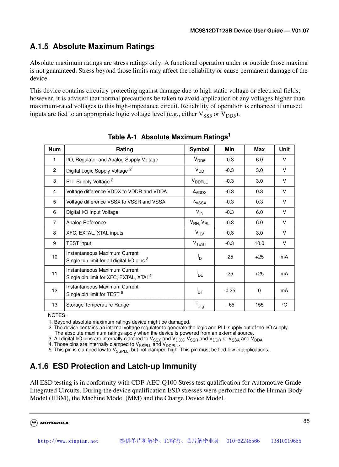
Absolute Maximum Ratings
Num Rating Symbol Min Max Unit
ESD Protection and Latch-up Immunity
Table A-1 Absolute Maximum Ratings1
Model Description Symbol Value Unit
Table A-3 ESD and Latch-Up Protection Characteristics
Operating Conditions
Table A-2 ESD and Latch-up Test Conditions
Rating Symbol Min Typ Max Unit
Power Dissipation and Thermal Characteristics
Table A-4 Operating Conditions
Pint = IDD ⋅ VDD + Iddpll ⋅ Vddpll + Idda ⋅ Vdda
Table A-5 Thermal Package Characteristics1
9 I/O Characteristics
Num Rating Symbol Min Typ Max Unit
Table A-6 5V I/O Characteristics
Measurement Conditions
Supply Currents
Additional Remarks
Table A-7 Supply Current Characteristics
ATD Operating Characteristics
ATD Characteristics
Table A-8 ATD Operating Characteristics
Factors influencing accuracy
Source capacitance
Table A-9 ATD Electrical Characteristics
Current injection
Table A-10 ATD Conversion Performance
ATD accuracy
Figure A-1 ATD Accuracy Definitions
NVM timing
NVM, Flash and Eeprom
Single Word Programming
Burst Programming
Sector Erase
Table A-11 NVM Timing Characteristics
Mass Erase
Blank Check
NVM Reliability
Table A-12 NVM Reliability Characteristics
Num Rating Cycles Data Retention Unit Lifetime
100
Table A-13 Voltage Regulator Recommended Load Capacitances
Voltage Regulator
102
Startup
Reset, Oscillator and PLL
Table A-15 Oscillator Characteristics
Pseudo Stop and Wait Recovery
Oscillator
XFC Pin
Phase Locked Loop
XFC Component Selection
Jitter Information
⋅ synr +
= max ⎜ ⋅ t nom
Table A-16 PLL Characteristics
Mscan
Table A-17 Mscan Wake-up Pulse Characteristics
110
Master Mode
LSB Master LSB OUT
Mosi Port Data
Slave Mode
Table A-19 SPI Slave Mode Timing Characteristics
General Muxed Bus Timing
External Bus Timing
PA, PB
Eclk PE4
ECS PK7 PE2 Lstrb PE3 Noacc PE7 PIPO0
Pweh
Table A-20 Expanded Bus Timing Characteristics
118
Appendix B Package Information
112-pin Lqfp package
112-pin Lqfp mechanical dimensions case no
80-pin QFP package
80-pin QFP Mechanical Dimensions case no B
122
User Guide End Sheet
124