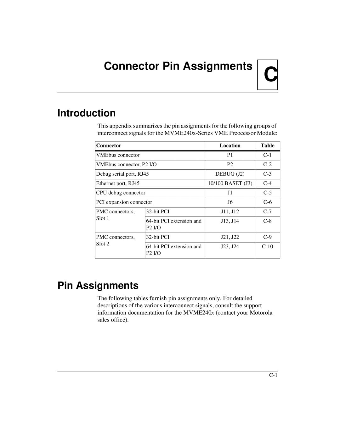
Connector Pin Assignments
C
Introduction
This appendix summarizes the pin assignments for the following groups of interconnect signals for the
Connector |
| Location | Table | |
|
|
|
| |
VMEbus connector |
| P1 | ||
|
|
| ||
VMEbus connector, P2 I/O | P2 | |||
|
|
| ||
Debug serial port, RJ45 | DEBUG (J2) | |||
|
|
|
| |
Ethernet port, RJ45 |
| 10/100 BASET (J3) | ||
|
|
|
| |
CPU debug connector |
| J1 | ||
|
|
| ||
PCI expansion connector | J6 | |||
|
|
|
| |
PMC connectors, |
| J11, J12 | ||
Slot 1 |
|
|
|
|
| J13, J14 | |||
|
| |||
|
| P2 I/O |
|
|
|
|
|
|
|
PMC connectors, |
| J21, J22 | ||
Slot 2 |
|
|
|
|
| J23, J24 | |||
|
| |||
|
| P2 I/O |
|
|
|
|
|
|
|
Pin Assignments
The following tables furnish pin assignments only. For detailed descriptions of the various interconnect signals, consult the support information documentation for the MVME240x (contact your Motorola sales office).