MVME2400-Series Single Board Computer Installation and Use
Restricted Rights Legend
Memory Handles
Model
Document Terminology
Equipment. Use extreme caution when handling, testing,
Safety Summary Safety Depends On You
Page
Page
Page
Contents
Functional Description
Programming the MVME240x
Glossary
List of Figures
Xiv
List of Tables
Xvi
MVME240x Description
Introduction
MVME240x Models
MVME240x Module
Expansion Module Description
PMCspan Expansion Mezzanine
PCI Mezzanine Cards PMCs
PMCspan Models
Start-Up Overview
Overview of Start-Up Procedures
VMEsystem Enclosure
System Console Terminal
PMCspan
Installing the MVME240x Hardware Status Indicators
Unpacking the MVME240x Hardware
Preparing the MVME240x Hardware
MVME240x
Preparing and Installing the MVME2400-Series Module
MVME240xPreparing theHardware
ConnectorsHeaders,MFVME240xigure 1-1.Switches, LEDs
Setting the VMEbus System Controller Selection Header J9
General-Purpose Software-Readable Header
PMCspan
PMCs
ESD Precautions
Installing the MVME240x Hardware
Preparing and Installing the MVME2400-Series Module
Typical Single-width PMC Module Placement on MVME240x
Primary PMCspan
PMCspan-002 Installation on an MVME240x
Secondary PMCspan
PMCspan-010 Installation onto a PMCspan-002/MVME240x
Preparing and Installing the MVME2400-Series Module
MVME240x
Preparing and Installing the MVME2400-Series Module
Installation Considerations
Preparing and Installing the MVME2400-Series Module
Operating Instructions
Applying Power
MVME240x
Switches
RST S2
ABT S1
PMC1 DS4
Status Indicators
10/100 Baset Port
PMC2 DS3
MVME240x
Debug Port
MVME240x Debug Port Configuration
PCI Mezzanine Card PMC Slot
PMC Slots
PMCspan
Features
MVME240x Features
Feature Description
VME I/O
Features
Block Diagram
General Description
MPC750 Processor
MVME240x Block Diagram
L2 Cache
Power Requirements
Hawk System Memory Controller SMC/PCI Host Bridge PHB Asic
PCI Bus Latency
PCI Originated Latency Matrix
PCI Originated Bandwidth Matrix
PPC Bus Latency
PPC60x Originated Latency Matrix
PPC60x Originated Bandwidth Matrix
Assumptions
PPC60x Originated
Clock Ratios and Operating Frequencies
PCI Originated
Sdram Memory
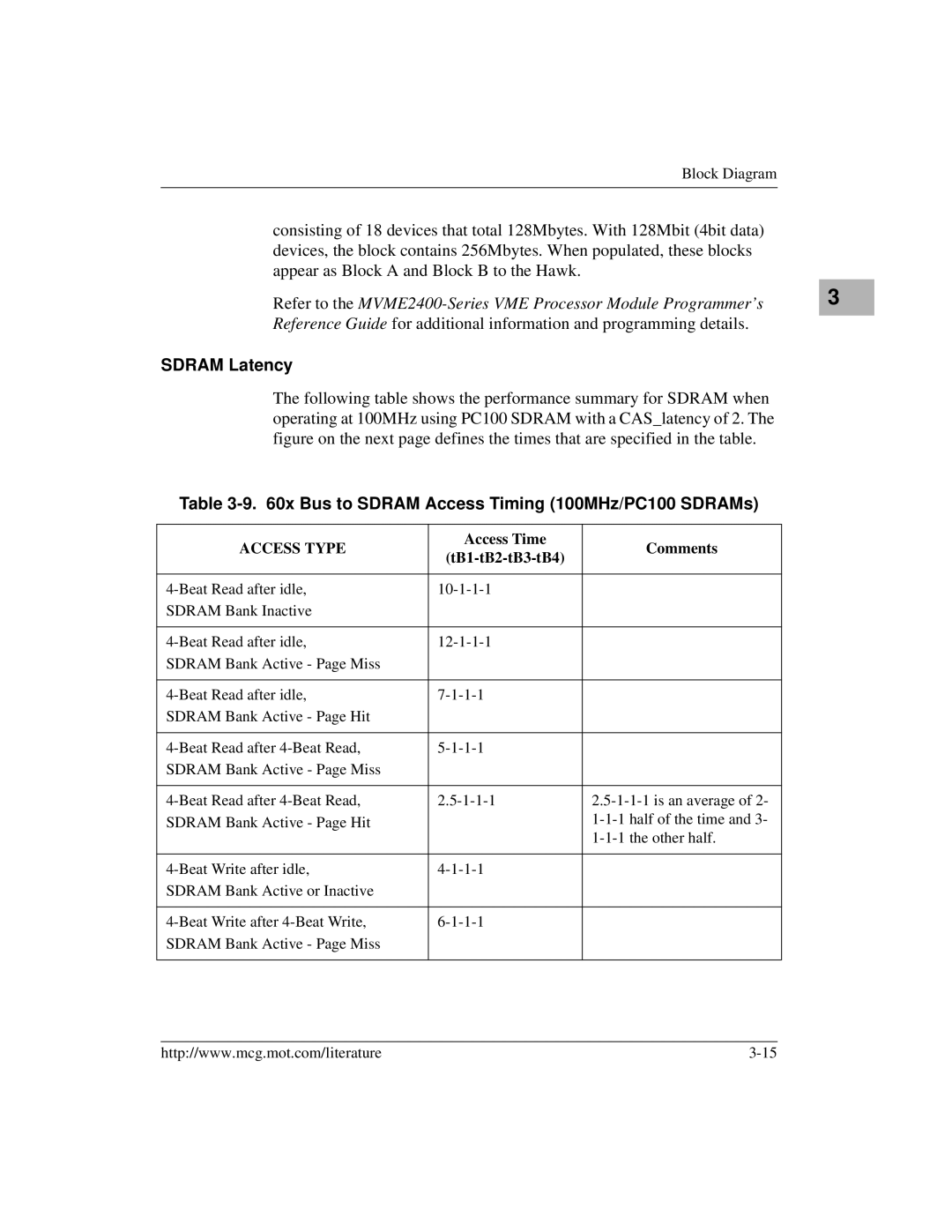
X Bus to Sdram Access Timing 100MHz/PC100 SDRAMs
Access Time Comments TB1-tB2-tB3-tB4
Sdram Latency
X Bus to Sdram Access Timing 100MHz/PC100 SDRAMs
Timing Definitions for PPC Bus to Sdram Access
Functional Description
ROM/Flash Performance
Flash Memory
1st Beat 2nd Beat 3rd Beat 4th Beat Clocks Bits
Total
1st Beat 2nd Beat 3rd Beat 4th Beat Bits
12. PPC Bus to ROM/Flash Access Timing 50ns @ 100MHz
Ethernet Interface
PMC Slot 1 Single-Width PMC
PCI Mezzanine Card PMC Interface
PMC Slot 2 Single-Width PMC
PMC Slots 1 and 2 Double-Width PMC
PCI Expansion
Asynchronous Debug Port
VMEbus Interface
PCI-ISA Bridge PIB Controller
PCI Host Bridge PHB
Real-Time Clock/NVRAM/Timer Function
Programmable Timers
Interval Timers
Interrupt Controller Mpic
16/32-Bit Timers
Page
Memory Maps
Programming the MVME240x
Default Processor Memory Map
Processor Default View of the Memory Map
Processor Bus Memory Map
VMEbus Memory Map
PCI Local Bus Memory Map
PCI Arbitration
Programming Considerations
VMEbus Master Mapping
Interrupt Handling
PCI Arbitration Assignments
PCI Bus Request PCI Masters
MVME240x Interrupt Architecture
DMA Channels
Sources of Reset
Asic
Classes of Reset and Effectiveness
Endian Issues
Processor/Memory Domain
PCI Domain
VMEbus Domain
Role of the Universe Asic
Page
PPCBug Basics
PPCBug Overview
PPCBug
MPU, Hardware, and Firmware Initialization
Memory Requirements
PPCBug Implementation
PPCBug
Using PPCBug
Debugger Commands
Command Description
Debugger Commands
Gevedit
NAB
Time
Diagnostic Tests
PPC4-Bug prompt
Test Group Description
Diagnostic Test Groups
Overview
Modifying the Environment
Cnfg Configure Board Information Block
ENV Set Environment
Configuring the PPCBug Parameters
Remote Start Method Switch G/M/B/N = B?
Select the identifier. Default =
Nvram Bootlist GEV.fw-boot-path Boot Enable Y/N = N?
Default = $00
ROM Boot Enable Y/N = N?
Network Auto Boot Enable Y/N = N?
Nvram
ROM Next Access Length 0 15 = 0?
Configuring the VMEbus Interface
PCI Slave Image 0 Control = 00000000?
PCI Slave Image 2 Bound Address Register = 22000000?
VMEbus Slave Image 1 Base Address Register = 00000000?
VMEbus Slave Image 3 Translation Offset = 00000000?
Motorola Computer Group Documents
Table A-1. Motorola Computer Group Documents
Document Title Publication Number
Manufacturers’ Documents
Table A-2. Manufacturers’ Documents
Document Title and Source Publication Number
Ordering Related Documentation
Table A-2. Manufacturers’ Documents
Table A-3. Related Specifications
Related Specifications
Related Specifications
ANSI/EIA-232-D
Page
Specifications
Table B-1. MVME240x Specifications
Characteristics Specifications
PMC I/O
Cooling Requirements
EMC Regulatory Compliance
Pin Assignments
Connector Location
VMEbus Connector P1
Table C-1. P1 VMEbus Connector Pin Assignments
Row Z Row a Row B Row C Row D
Connector Pin Assignments
Table C-2. P2 Connector Pin Assignment
VMEbus Connector P2
VPC
Table C-4 /100 Baset J3 Connector Pin Assignments
Serial Port Connector Debug J2
Ethernet Connector 10BASET J3
Table C-3. Debug J2Connector Pin Assignments
Table C-5. Debug Connector Pin Assignments
CPU Debug Connector J1
PD0 PD2 PD4 PD6 PD8
100 102 104 106 108 110 112 114
+3.3V
Table C-5. Debug Connector Pin Assignments
Table C-6. J6 PCI Expansion Connector Pin Assignments
PCI Expansion Connector J6
PAR
PAR64
PCI Mezzanine Card Connectors J11 through J14
Table C-7. J11 J12 PMC1 Connector Pin Assignments
J11 J12
J13 J14
Table C-8. J13 J14 PMC1 Connector Pin Assignments
PMC143 P2-C22 PMC144 P2-A22
PCI Mezzanine Card Connectors J21 through J24
Table C-9. J21 and J22 PMC2 Connector Pin Assignments
J21 J22
J23 J24
Table C-10. J23 and J24 PMC2 Connector Pin Assignments
PMC231 P2-D21 PMC232 P2-Z21
Table D-1. Troubleshooting MVME240x Modules
Solving Startup Problems
Solving Startup Problems
Troubleshooting the MVME240x
Troubleshooting Procedure Complete
Abbreviations, Acronyms, and Terms to Know
Glossary
O S S a R Y
Compact Disk Read-Only Memory
Dynamic Random Access Memory. a memory technology that is
Fiber Distributed Data Interface. a network based on the use
High
Ultra 603/Ultra 604 system board. It provides the necessary
Operating System. The software that manages the computer
IBM
Random-Access Memory. The temporary memory that a computer
Single Inline Memory Module. a small circuit board with RAM
UltraViolet
EXtended Graphics Array. An improved IBM VGA monitor
GL-14
Index
Dram
IN-3
PCI bus 3-4,3-23,3-26,4-3,4-6 PCI bus latency
PHB
Romnal
IN-7
Index
86 100 pages 5/16 spine
Cover Pages 1/8 spine