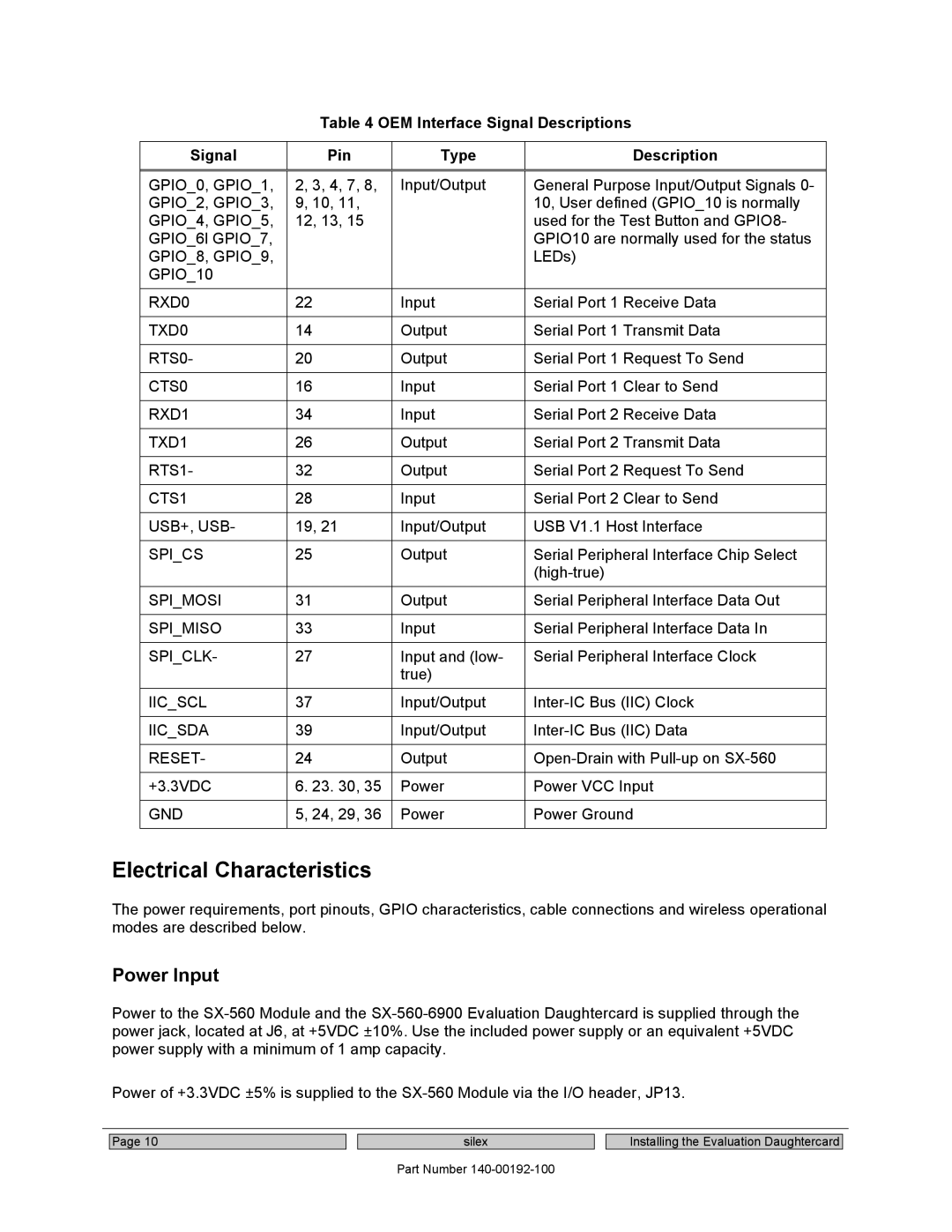
Table 4 OEM Interface Signal Descriptions
Signal | Pin | Type | Description |
|
|
|
|
GPIO_0, GPIO_1, | 2, 3, 4, 7, 8, | Input/Output | General Purpose Input/Output Signals 0- |
GPIO_2, GPIO_3, | 9, 10, 11, |
| 10, User defined (GPIO_10 is normally |
GPIO_4, GPIO_5, | 12, 13, 15 |
| used for the Test Button and GPIO8- |
GPIO_6l GPIO_7, |
|
| GPIO10 are normally used for the status |
GPIO_8, GPIO_9, |
|
| LEDs) |
GPIO_10 |
|
|
|
|
|
|
|
RXD0 | 22 | Input | Serial Port 1 Receive Data |
|
|
|
|
TXD0 | 14 | Output | Serial Port 1 Transmit Data |
|
|
|
|
RTS0- | 20 | Output | Serial Port 1 Request To Send |
|
|
|
|
CTS0 | 16 | Input | Serial Port 1 Clear to Send |
|
|
|
|
RXD1 | 34 | Input | Serial Port 2 Receive Data |
|
|
|
|
TXD1 | 26 | Output | Serial Port 2 Transmit Data |
|
|
|
|
RTS1- | 32 | Output | Serial Port 2 Request To Send |
|
|
|
|
CTS1 | 28 | Input | Serial Port 2 Clear to Send |
|
|
|
|
USB+, USB- | 19, 21 | Input/Output | USB V1.1 Host Interface |
|
|
|
|
SPI_CS | 25 | Output | Serial Peripheral Interface Chip Select |
|
|
| |
|
|
|
|
SPI_MOSI | 31 | Output | Serial Peripheral Interface Data Out |
|
|
|
|
SPI_MISO | 33 | Input | Serial Peripheral Interface Data In |
|
|
|
|
SPI_CLK- | 27 | Input and (low- | Serial Peripheral Interface Clock |
|
| true) |
|
|
|
|
|
IIC_SCL | 37 | Input/Output | |
|
|
|
|
IIC_SDA | 39 | Input/Output | |
|
|
|
|
RESET- | 24 | Output | |
|
|
|
|
+3.3VDC | 6. 23. 30, 35 | Power | Power VCC Input |
|
|
|
|
GND | 5, 24, 29, 36 | Power | Power Ground |
|
|
|
|
Electrical Characteristics
The power requirements, port pinouts, GPIO characteristics, cable connections and wireless operational modes are described below.
Power Input
Power to the
Power of +3.3VDC ±5% is supplied to the
Page 10
silex
Part Number
Installing the Evaluation Daughtercard
