OEM Interface
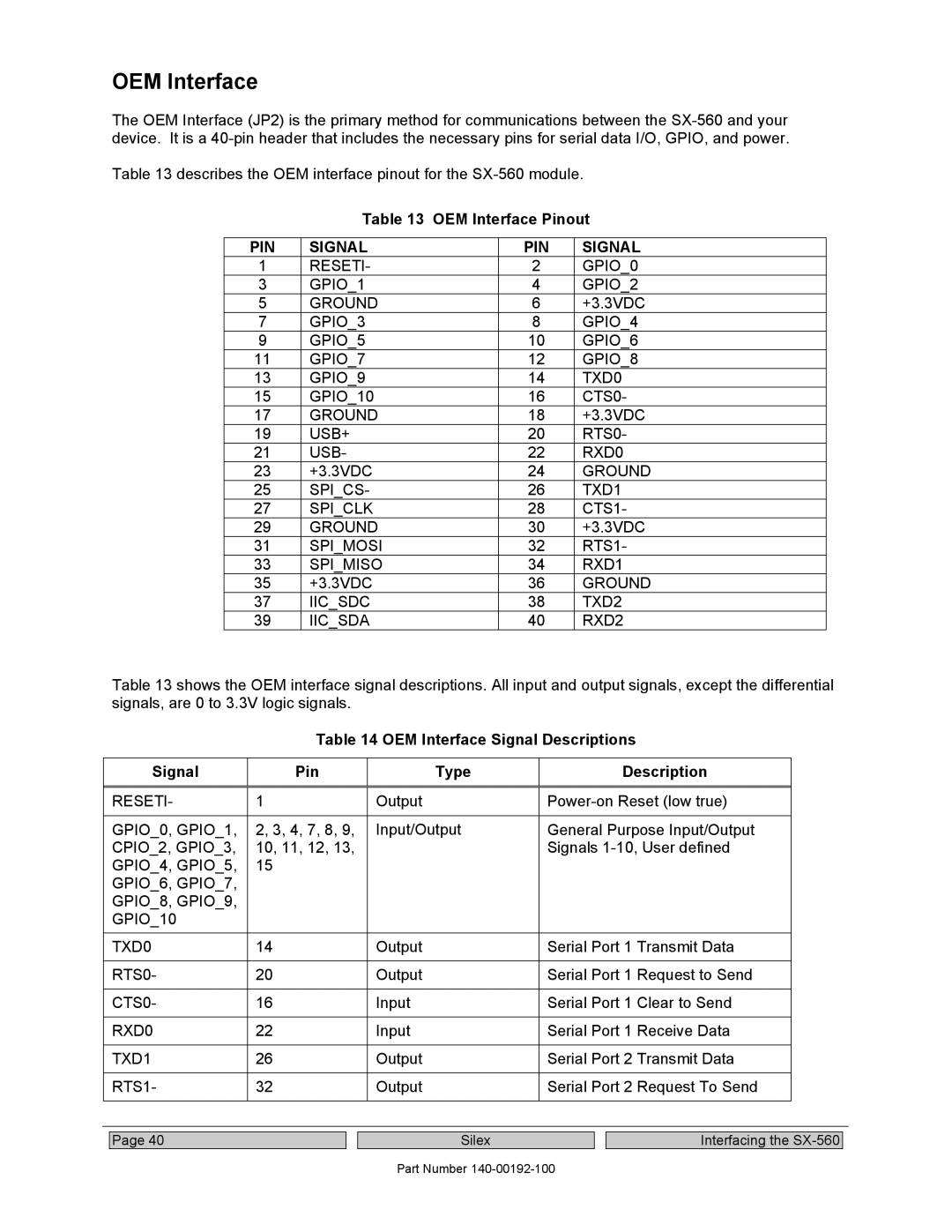
The OEM Interface (JP2) is the primary method for communications between the
Table 13 describes the OEM interface pinout for the
Table 13 OEM Interface Pinout
PIN | SIGNAL | PIN | SIGNAL |
1 | RESETI- | 2 | GPIO_0 |
3 | GPIO_1 | 4 | GPIO_2 |
5 | GROUND | 6 | +3.3VDC |
7 | GPIO_3 | 8 | GPIO_4 |
9 | GPIO_5 | 10 | GPIO_6 |
11 | GPIO_7 | 12 | GPIO_8 |
13 | GPIO_9 | 14 | TXD0 |
15 | GPIO_10 | 16 | CTS0- |
17 | GROUND | 18 | +3.3VDC |
19 | USB+ | 20 | RTS0- |
21 | USB- | 22 | RXD0 |
23 | +3.3VDC | 24 | GROUND |
25 | SPI_CS- | 26 | TXD1 |
27 | SPI_CLK | 28 | CTS1- |
29 | GROUND | 30 | +3.3VDC |
31 | SPI_MOSI | 32 | RTS1- |
33 | SPI_MISO | 34 | RXD1 |
35 | +3.3VDC | 36 | GROUND |
37 | IIC_SDC | 38 | TXD2 |
39 | IIC_SDA | 40 | RXD2 |
Table 13 shows the OEM interface signal descriptions. All input and output signals, except the differential signals, are 0 to 3.3V logic signals.
Table 14 OEM Interface Signal Descriptions
Signal | Pin | Type | Description | |
|
|
|
| |
RESETI- | 1 | Output | ||
|
|
|
| |
GPIO_0, GPIO_1, | 2, 3, 4, 7, 8, 9, | Input/Output | General Purpose Input/Output | |
CPIO_2, GPIO_3, | 10, 11, 12, 13, |
| Signals | |
GPIO_4, GPIO_5, | 15 |
|
|
|
GPIO_6, GPIO_7, |
|
|
|
|
GPIO_8, GPIO_9, |
|
|
|
|
GPIO_10 |
|
|
|
|
|
|
|
| |
TXD0 | 14 | Output | Serial Port 1 Transmit Data | |
|
|
|
| |
RTS0- | 20 | Output | Serial Port 1 Request to Send | |
|
|
|
|
|
CTS0- | 16 | Input | Serial Port 1 | Clear to Send |
|
|
|
|
|
RXD0 | 22 | Input | Serial Port 1 | Receive Data |
|
|
|
|
|
TXD1 | 26 | Output | Serial Port 2 | Transmit Data |
|
|
|
|
|
RTS1- | 32 | Output | Serial Port 2 | Request To Send |
|
|
|
|
|
Page 40
Silex
Part Number
Interfacing the
