TNETX3270
ThunderSWITCH 24/3 ETHERNET SWITCH
WITH 24 10-MBIT/S PORTS AND 3 10-/100-MBIT/S PORTS
SPWS043B ± NOVEMBER 1997 ± REVISED APRIL 1999
EEPROM interface
The EEPROM interface is provided so the
The EEPROM contains configuration and initialization information that are accessed infrequently, typically at power up and after a reset. The organization of the EEPROM data is in accordance with the DIO address map.
EEPROM downloads can be initiated in one of two ways:
DAt the end of hard reset (rising edge on RESET, or completion of a DIO write to DIOaddrhi register that changes the value of the three most significant bits from 010 to another value).
DWriting a 1 to load in Syscontrol register. This bit is cleared automatically when the download completes. It cannot be set during the download by the EEPROM data, thereby preventing a download loop.
During the download, no DIO writes are permitted. If a DIO write is attempted, SRDY is held high until the download has completed.
The EEPROM size is detected automatically according to the address assigned to the EEPROM:
D2048 bits organized as a 256 ⋅ 8 EEPROM should have its A0, A1, and A2 pins tied low.
D8192 bits organized as a 1024 ⋅ 8 EEPROM should have its A0 and A1 pins tied low and A2 pin tied high.
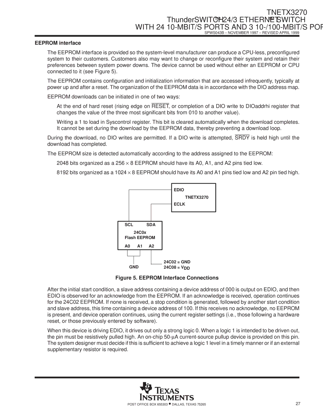
EDIO
TNETX3270
ECLK
SCL |
|
| SDA |
| ||
|
| 24C0x |
|
|
| |
Flash EEPROM |
| |||||
A0 | A1 | A2 |
| |||
|
|
|
|
|
| 24C02 = GND |
|
|
|
|
|
| |
|
|
|
|
|
| |
| GND |
|
| 24C08 = VDD | ||
Figure 5. EEPROM Interface Connections
After the initial start condition, a slave address containing a device address of 000 is output on EDIO, and then EDIO is observed for an acknowledge from the EEPROM. If an acknowledge is received, operation continues for the 24C02 EEPROM. If none is received, a stop condition is generated, followed by another start condition and slave address, this time containing a device address of 100. If this receives no acknowledge, no EEPROM is present, and device operation continues, using the current register settings (i.e., those following a hardware reset, or those previously entered by software).
When this device is driving EDIO, it drives out only a strong logic 0. When a logic 1 is intended to be driven out, the pin must be resistively pulled high. An
POST OFFICE BOX 655303 •DALLAS, TEXAS 75265 | 27 |