TNETX3270
ThunderSWITCH 24/3 ETHERNET SWITCH
WITH 24 10-MBIT/S PORTS AND 3 10-/100-MBIT/S PORTS
SPWS043B ± NOVEMBER 1997 ± REVISED APRIL 1999
PARAMETER MEASUREMENT INFORMATION
Outputs are driven to a minimum
Output transition times are specified as follows: For a
The rise and fall times are not specified but are assumed to be those of standard TTL devices, which are typically 1.5 ns.
2 V (high)
1.4 V
0.8 V (low)
test measurement
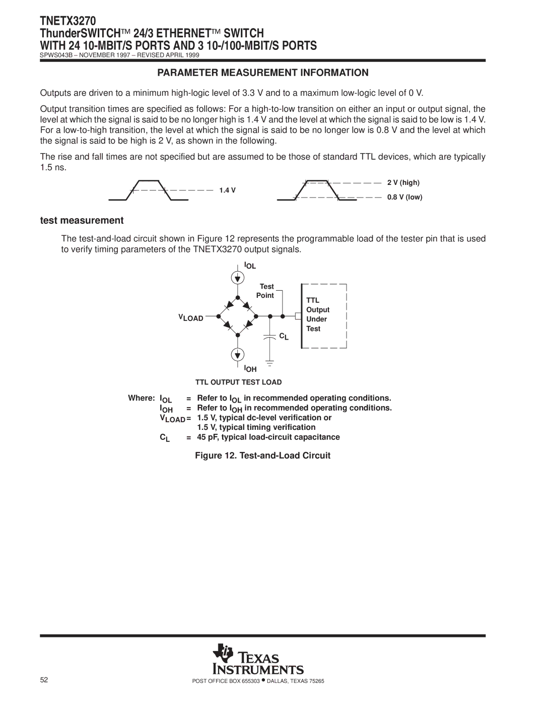
The
IOL
Test
Point
VLOAD
CL
TTL
Output
Under
Test
|
|
| IOH |
|
| TTL OUTPUT TEST LOAD | |
Where: IOL | = | Refer to IOL in recommended operating conditions. | |
IOH | = | Refer to IOH in recommended operating conditions. | |
VLOAD = | 1.5 | V, typical | |
|
| 1.5 | V, typical timing verification |
CL | = | 45 pF, typical | |
Figure 12. Test-and-Load Circuit
52 | POST OFFICE BOX 655303 •DALLAS, TEXAS 75265 |